NB2304AI1DR2G

Semiconductor Components Industries, LLC, 2010
October, 2010 -- Rev. 9
1 Publication Order Number:
NB2304A/D
NB2304A
3.3 V Zero Delay
Clock Buffer
The NB2304A is a versatile, 3.3 V zero delay buffer designed to
distribute high--speed clocks in PC, workstation, datacom, telecom
and other high--performance applications. It is available in an 8 pin
package. The part has an on--chip PLL which locks to an input clock
presented on the REF pin. The PLL feedback is required to be driven
to FBK pin, and can be obtained from one of the outputs. The
input--to--output propagation delay is guaranteed to be less than
250 ps, and the output--to--output skew is guaranteed to be less than
200 ps.
The NB2304A has two Banks of two outputs each. Multiple
NB2304A devices can accept the same input clock and distribute it. In
this case, the skew between the outputs of the two devices is
guaranteed to be less than 500 ps.
The NB2304A is available in two different configurations (Refer to
NB2304A Configurations Table). The NB2304AI1 is the base part,
where the output frequencies equal the reference if there is no counter
in the feedback path. The NB2304AI1H is the high--drive version of
the --1 and the rise and fall times on this device are much faster.
The NB2304AI2 allows the user to obtain REF, 1/2 X and 2X
frequencies on each output Bank. The exact configuration and output
frequencies depend on which output drives the feedback pin.
Features
Zero Input -- Output Propagation Delay, Adjustable by Capacitive
Load on FBK Input
Multiple Configurations -- Refer to NB2304A Configurations Table
Input Frequency Range: 15 MHz to 133 MHz
Multiple Low--Skew Outputs
Output--Output Skew < 200 ps
Device--Device Skew < 500 ps
Two Banks of Four Outputs
Less than 200 ps Cycle--to--Cycle Jitter (--1, --1H, --5H)
Available in Space Saving, 8 pin 150 mil SOIC Package
3.3 V Operation
Advanced 0.35 m CMOS Technology
Guaranteed Across Commercial and Industrial Temperature Ranges
These are Pb--Free Devices
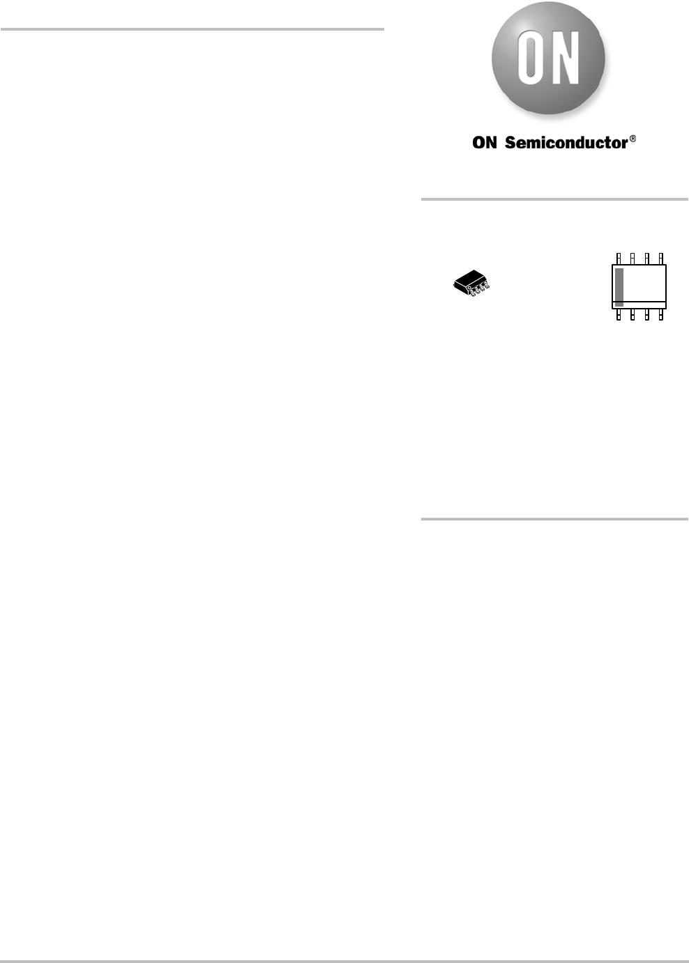
MARKING
DIAGRAM*
XXXX = Device Code
A = Assembly Location
L = Wafer Lot
Y = Year
W = Work Week
G = Pb --Free Package
*For additional marking information, refer to
Application Note AND8002/D.
SOIC--8
D SUFFIX
CASE 751
See detailed orderingandshipping informationinthepackage
dimensions section on page 6 of this data sheet.
ORDERING INFORMATION
http://onsemi.com
1
8
XXXX
ALYW
G
1
8
NB2304A
http://onsemi.com
2
Figure 1. Basic Block Diagram
(see Figures 11 and 12 for device specific Block Diagrams)
FBK
CLKA1
CLKA2
CLKB1
CLKB2
REF
PLL
Extra Divider (--2)÷2
Table 1. CONFIGURATIONS
Device Feedback From Bank A Frequency Bank B Frequency
NB2304AI1 Bank A or Bank B Reference Reference
NB2304AI1H Bank A or Bank B Reference Reference
NB2304AI2 Bank A Reference Reference ÷2
NB2304AI2 Bank B 2 X Reference Reference
Figure 2. Pin Configuration
V
DD
1
2
3
4
8
7
6
5
REF
CLKA1
CLKA2
GND
FBK
CLKB2
CLKB1
NB2304A
Table 2. PIN DESCRIPTION
Pin # Pin Name Description
1 REF (Note 1) Input reference frequency, 5 V
tolerant input.
2 CLKA1 (Note 2) Buffered clock output, Bank A.
3 CLKA2 (Note 2) Buffered clock output, Bank A.
4 GND Ground.
5 CLKB1 (Note 2) Buffered clock output, Bank B.
6 CLKB2 (Note 2) Buffered clock output, Bank B.
7 V
DD
3.3 V supply.
8 FBK PLL feedback input.
1. Weak pulldown.
2. Weak pulldown on all outputs.
NB2304A
http://onsemi.com
3
Table 3. MAXIMUM RATINGS
Parameter Min Max Unit
Supply Voltage to Ground Potential -- 0 . 5 +7.0 V
DC Input Voltage (Except REF) -- 0 . 5 V
DD
+0.5 V
DC Input Voltage (REF) -- 0 . 5 7 V
Storage Temperature -- 6 5 +150 C
Maximum Soldering Temperature (10 sec) 260 C
Junction Temperature 150 C
Static Discharge Voltage (per MIL--STD--883, Method 3015) > 2000 V
Stresses exceeding Maximum Ratings may damage the device. Maximum Ratings are stress ratings only. Functional operation above the
Recommended Operating Conditions is not implied. Extended exposure to stresses above the Recommended Operating Conditions may affect
device reliability.
Table 4. OPERATING CONDITIONS
Parameter Description Min Max Unit
V
DD
Supply Voltage 3.0 3.6 V
T
A
Operating Temperature (Ambient Temperature) Industrial
Commercial
-- 4 0
0
85
70
C
C
L
Load Capacitance, 15 MHz to 100 MHz 30 pF
C
L
Load Capacitance, from 100 MHz to 133 MHz 15 pF
C
IN
Input Capacitance (Note 3) 7 pF
3. Applies to both REF Clock and FBK.
Table 5. ELECTRICAL CHARACTERISTICS V
CC
= 3.0 V to 3.6 V, GND = 0 V, T
A
=--40Cto+85C
Parameter
Description Test Conditions Min Max Unit
V
IL
Input LOW Voltage 0.8 V
V
IH
Input HIGH Voltage 2.0 V
I
IL
Input LOW Current V
IN
=0V 50.0
mA
I
IH
Input HIGH Current V
IN
=V
DD
100.0
mA
V
OL
Output LOW Voltage I
OL
= 8 mA (--1, --2)
I
OL
=12mA(--1H)
0.4 V
V
OH
Output HIGH Voltage I
OH
= --8 mA (--1, --2)
I
OH
=--12mA(--1H)
2.4 V
I
DD
Supply Current
Unloaded outputs 100 MHz REF
Select inputs at V
DD
or GND
45
mA
Unloaded outputs, 66 MHz REF ( --1, --2) 35
Unloaded outputs, 33 MHz REF ( --1, --2) 20

NB2304AI1DR2G

Mfr. #:
Manufacturer:
ON Semiconductor
Description:
Phase Locked Loops - PLL 3.3V Quad Output Zero Delay Buffer
Lifecycle:
New from this manufacturer.
Delivery:
DHL FedEx Ups TNT EMS
Payment:
T/T Paypal Visa MoneyGram Western Union