NB2304AI1DR2G

NB2304A
http://onsemi.com
4
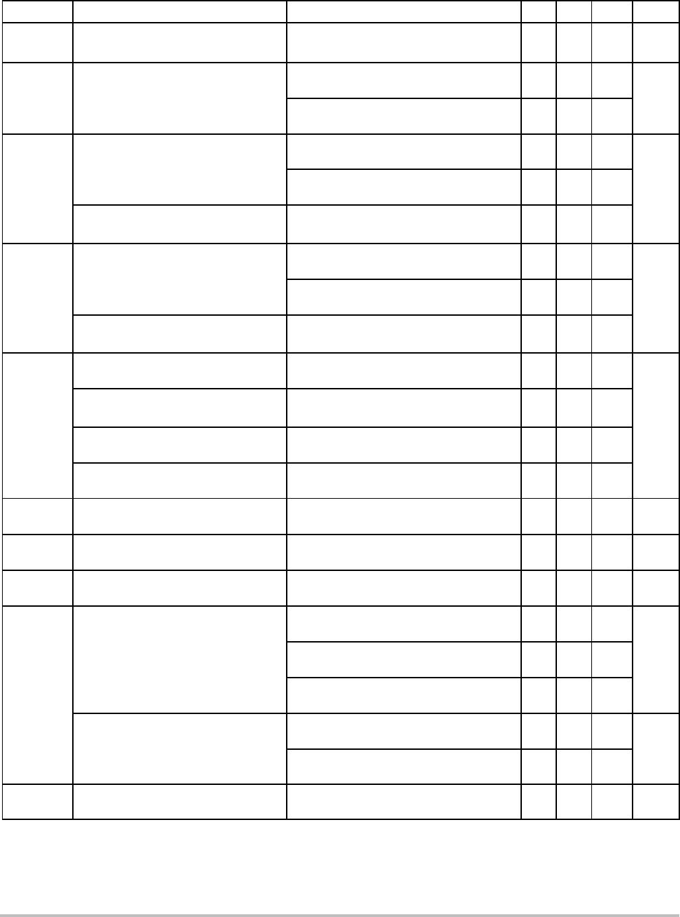
Table 6. SWITCHING CHARACTERISTICS V
CC
= 3.0 V to 3.6 V, GND = 0 V, T
A
=--40Cto+85C
(All parameters are specified with loaded outputs)
Parameter
Description Test Conditions Min Typ Max Unit
t
1
Output Frequency 30 pF load (all devices)
15 pF load (--1, --2)
15
15
100
133.3
MHz
t
1
Duty Cycle = (t
2
/t
1
) * 100
(all devices)
Measured at 1.4 V, F
OUT
66.66 MHz
30 pF load
40.0 50.0 60.0
%
Measured at 1.4 V, F
OUT
50 MHz
15 pF load
45.0 50.0 55.0
t
3
Output Rise Time
(--1, --2)
Measured between 0.8 V and 2.0 V
30 pF load
2.50
ns
Measured between 0.8 V and 2.0 V
15 pF load
1.50
Output Rise Time
(--1H)
Measured between 0.8 V and 2.0 V
30 pF load
1.50
t
4
Output Fall Time
(--1, --2)
Measured between 2.0 V and 0.8 V
30 pF load
2.50
ns
Measured between 2.0 V and 0.8 V
15 pF load
1.50
Output Fall Time
(--1H)
Measured between 2.0 V and 0.8 V
30 pF load
1.25
t
5
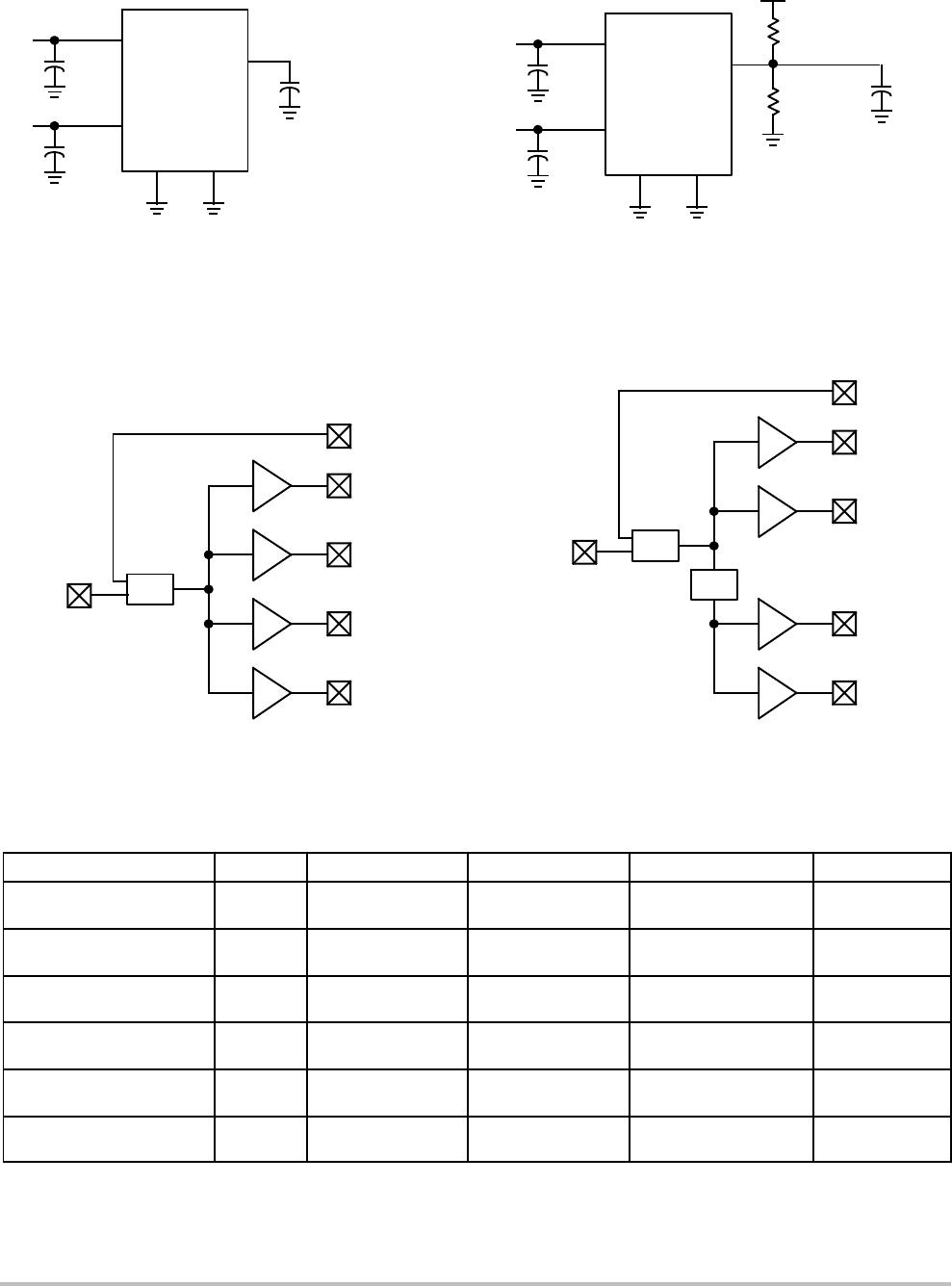
Output--to--Output Skew on same Bank
(--1, --2)
All outputs equally loaded 200
ps
Output--to--Output Skew
(--1H)
All outputs equally loaded 200
Output Bank A--to--Output Bank B skew
(--1)
All outputs equally loaded 200
Output Bank A--to--Output Bank B skew
(--2)
All outputs equally loaded 400
t
6
Delay, REF Rising Edge to FBK Rising
Edge
Measured at V
DD
/2 0 250 ps
t
7
Device--to-- Device Skew Measured at V
DD
/2 on the FBK pins of the
device
0 500 ps
t
8
Output Slew Rate Measured between 0.8 V and 2.0 V using
Test Circuit # 2
1 V/ns
t
J
Cycle--to--Cycle Jitter
(--1, --1H)
Measured at 66.67 MHz, loaded outputs,
15 pF load
180
ps
Measured at 66.67 MHz, loaded outputs,
30 pF load
200
Measured at 133.3 MHz, loaded outputs,
15 pF load
100
Cycle--to--Cycle Jitter
(--2)
Measured at 66.67 MHz, loaded outputs,
30 pF load
400
ps
Measured at 66.67 MHz, loaded outputs,
15 pF load
380
t
LOCK
PLL Lock Time Stable power supply, valid clock presented
on REF and FBK pins
1.0 ms
NB2304A
http://onsemi.com
5
Zero Delay and Skew Control
For applications requiring zero input--output delay, all
outputs must be equally loaded.
Figure 3. REF Input to CLKA/CLKB Delay vs.
Difference in Loading between FBK Pin and
CLKA/CLKB Pins
1500
1000
500
0
--500
--1000
--1500
-- 3 0 -- 2 5 -- 2 0 -- 1 5 -- 1 0 -- 5 0 5 1 0 1 5 2 0 2 5 3 0
REF INPUT TO CLKA/CLKB DELA
Y
(ps)
OUTPUT LOAD DIFFERENCE: FBK LOAD -- CLKA/CLKB LOAD (pF)
To close the feedback loop of the NB2304A, the FBK pin
can be driven from any of the four available output pins. The
output driving the FBK pin will be driving a total load of
7 pF plus any additional load that it drives. The relative
loading of this output (with respect to the remaining outputs)
can adjust the input output delay. This is shown in Figure 3.
For applications requiring zero input--output delay, all
outputs including the one providing feedback should be
equally loaded. If input--output delay adjustments are
required, use Figure 3 to calculate loading differences
between the feedback output and remaining outputs. For
zero output--output skew, be sure to load outputs equally.
SWITCHING WAVEFORMS
Figure 4. Duty Cycle Timing
1.4 V 1.4 V 1.4 V
t
1
t
2
Figure 5. All Outputs Rise/Fall Time
t
3
OUTPUT
2.0 V
0.8 V
t
4
2.0 V
0.8 V
3.3 V
0V
1.4 V
1.4 V
t
5
Figure 6. Output -- Output Skew
OUTPUT
OUTPUT
t
6
INPUT
OUTPUT
Figure 7. Input -- Output Propagation Delay
V
DD
2
V
DD
2
Figure 8. Device -- Device Skew
t
7
FBK_Device 1
V
DD
2
V
DD
2
FBK_Device 2
NB2304A
http://onsemi.com
6
V
DD
V
DD
C
LOAD
GND GND
OUTPUTS
Figure 9. Test Circuit #1
10 pF
0.1 mF
0.1 mF
V
DD
V
DD
GND GND
OUTPUTS
0.1 mF
0.1 mF
1kΩ
1kΩ
Figure 10. Test Circuit #2
For parameter t
8
(output slew rate) on --1H devices
V
DD
TEST CIRCUITS
Figure 11. NB2304AI1 and NB2304AI1H
FBK
CLKA1
CLKA2
CLKB1
CLKB2
REF
PLL
Figure 12. NB2304AI2
FBK
CLKA1
CLKA2
CLKB1
CLKB2
REF
PLL
÷2
BLOCK DIAGRAMS
ORDERING INFORMATION
Device Marking Operating Range Package Shipping
Availability
NB2304AI1DG 4I1 Industrial &
Commercial
SOIC--8
(Pb--Free)
98 Units / Rail
Now
NB2304AI1DR2G 4I1 Industrial &
Commercial
SOIC--8
(Pb--Free)
2500 Tape & Reel
Now
NB2304AI1HDG 4I1H Industrial &
Commercial
SOIC--8
(Pb--Free)
98 Units / Rail
Now
NB2304AI1HDR2G 4I1H Industrial &
Commercial
SOIC--8
(Pb--Free)
2500 Tape & Reel
Now
NB2304AI2DG 4I2 Industrial &
Commercial
SOIC--8
(Pb--Free)
98 Units / Rail
Now
NB2304AI2DR2G 4I2 Industrial &
Commercial
SOIC--8
(Pb--Free)
2500 Tape & Reel
Now
For information on tape and reel specifications, including part orientation and tape sizes, please refer to our Tape and Reel Packaging
Specifications Brochure, BRD8011/D.

NB2304AI1DR2G

Mfr. #:
Manufacturer:
ON Semiconductor
Description:
Phase Locked Loops - PLL 3.3V Quad Output Zero Delay Buffer
Lifecycle:
New from this manufacturer.
Delivery:
DHL FedEx Ups TNT EMS
Payment:
T/T Paypal Visa MoneyGram Western Union