10
COMMERCIAL, INDUSTRIAL AND MILITARY
TEMPERATURE RANGES
IDT7203/7204/7205/7206/7207/7208 CMOS ASYNCHRONOUS FIFO
2,048 x 9, 4,096 x 9, 8,192 x 9, 16,384 x 9, 32,768 x 9 and 65,536 x 9
IDT
7203
7204
7205
7206
7207
7208
XI XI
9
18
9
WRITE (W)
FULL FLAG (FF)
RESET (RS)
9918
HFHF
DATA (D)
IN
READ (R)
EMPTY FLAG (EF)
RETRANSMIT (RT)
DATA
(Q)
OUT
IDT
7203
7204
7205
7206
7207
7208
2661 drw15
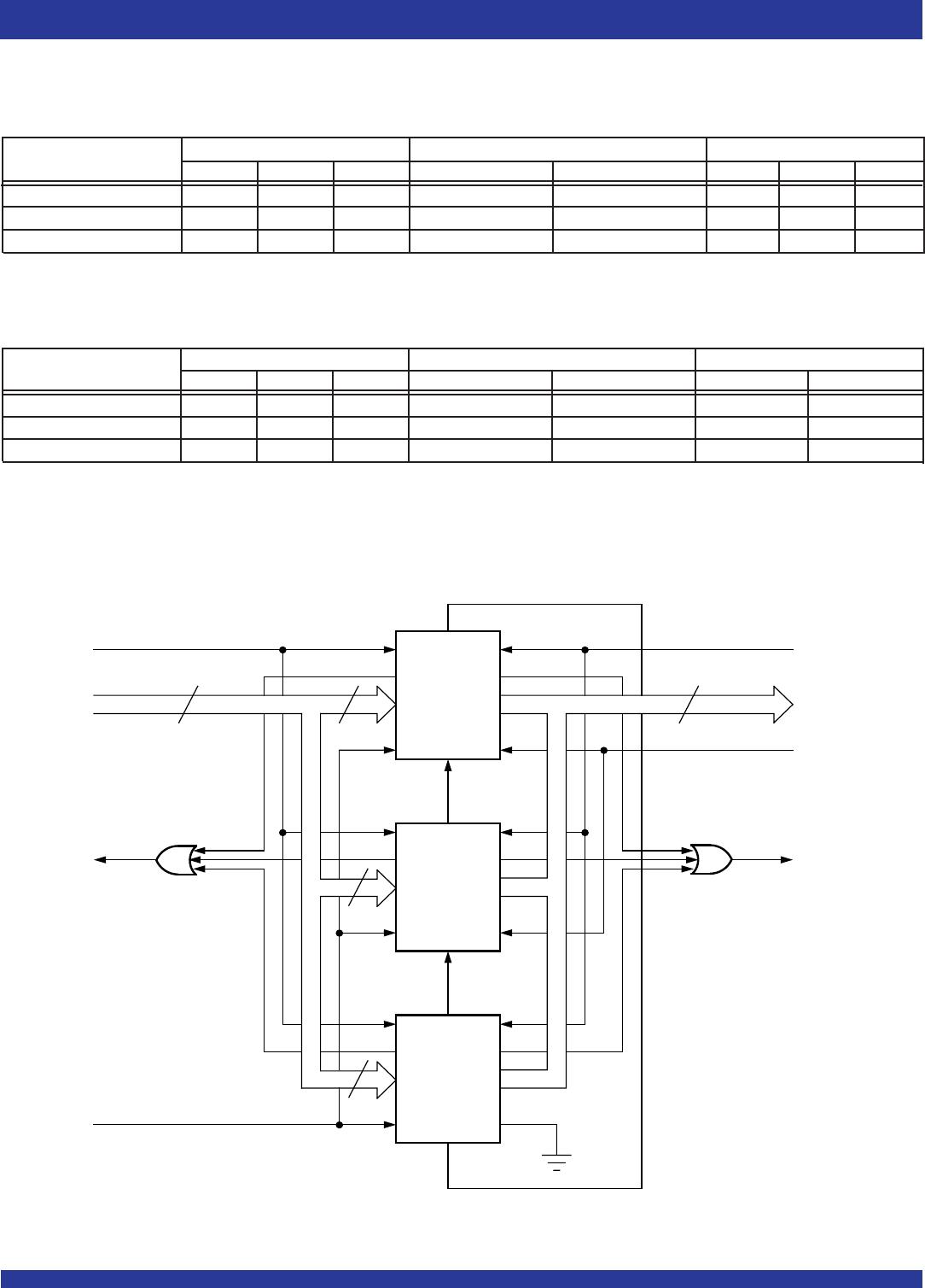
USAGE MODES:
Width Expansion
Word width may be increased simply by connecting the corresponding input
control signals of multiple devices. Status flags (EF, FF and HF) can be detected
from any one device. Figure 13 demonstrates an 18-bit word width by using
two IDT7203/7204/7205/7206/7207/7208s. Any word width can be attained
by adding additional IDT7203/7204/7205/7206/7207/7208s (Figure 13).
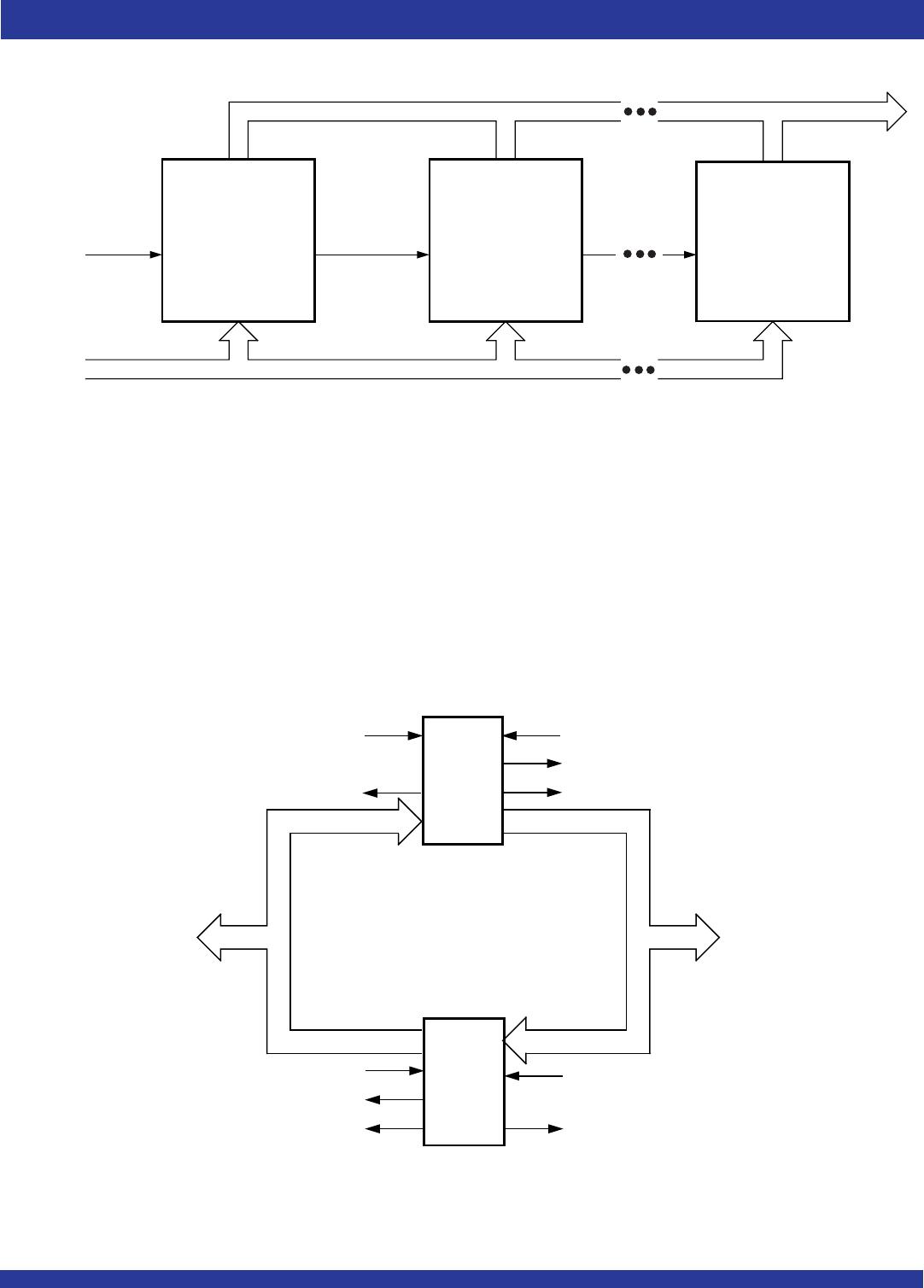
Bidirectional Operation
Applications which require data buffering between two systems (each
system capable of Read and Write operations) can be achieved by pairing
IDT7203/7204/7205/7206/7207/7208s as shown in Figure 16. Both Depth
Expansion and Width Expansion may be used in this mode.
Data Flow-Through
Two types of flow-through modes are permitted, a read flow-through and
write flow-through mode. For the read flow-through mode (Figure 17), the
FIFO permits a reading of a single word after writing one word of data into an
empty FIFO. The data is enabled on the bus in (tWEF + tA) ns after the rising
edge of W, called the first write edge, and it remains on the bus until the R line
is raised from LOW-to-HIGH, after which the bus would go into a three-state
mode after tRHZ ns. The EF line would have a pulse showing temporary
deassertion and then would be asserted.
In the write flow-through mode (Figure 18), the FIFO permits the writing of
a single word of data immediately after reading one word of data from a full FIFO.
The R line causes the FF to be deasserted but the W line being LOW causes
it to be asserted again in anticipation of a new data word. On the rising edge of
W, the new word is loaded in the FIFO. The W line must be toggled when FF
is not asserted to write new data in the FIFO and to increment the write pointer.
Compound Expansion
The two expansion techniques described above can be applied together
in a straightforward manner to achieve large FIFO arrays (see Figure 15).
NOTE:
1. Flag detection is accomplished by monitoring the FF, EF and HF signals on either (any) device used in the width expansion configuration.
Do not connect any output signals together.
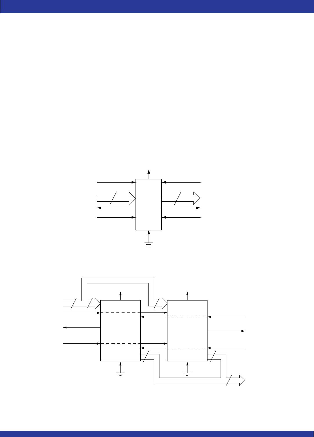
Figure 12. Block Diagram of 2,048 x 9, 4,096 x 9, 8,192 x 9, 16,384 x 9, 32,768 x 9, 65,536 x 9 FIFO Used in Single Device Mode
WRITE (W)
DATA IN (D)
FULL FLAG (FF)
RESET (RS)
9
READ (R)
9
DATA OUT (Q)
EMPTY FLAG (EF)
RETRANSMIT (RT)
EXPANSION IN (XI)
(HF)
IDT
7203
7204
7205
7206
7207
7208
(HALF-FULL FLAG)
2661 drw14
Figure 13. Block Diagram of 2,048 x 18, 4,096 x 18, 8,192 x 18, 16,384 x 18, 32,768 x 18, 65,536 x 18 FIFO Memory Used in Width Expansion Mode