AUGUST 2001 - REVISED JANUARY 2007
Specifications are subject to change without notice.
Customers should verify actual device performance in their specific applications.
TISP4xxxM3AJ Overvoltage Protector Series
These devices are two terminal overvoltage protectors. They may be used either singly to limit the voltage between two conductors (Figure 12)
or in multiples to limit the voltage at several points in a circuit (Figure 13).
APPLICATIONS INFORMATION
Deployment
Impulse Testing
To verify the withstand capability and safety of the equipment, standards require that the equipment is tested with various impulse wave forms.
The table below shows some common values.
In Figure 12, protector Th1 limits the maximum voltage between the two conductors to ±V
(BO)
. This configuration is normally used to protect
circuits without a ground reference, such as modems. In Figure 13, protectors Th2 and Th3 limit the maximum voltage between each conduc-
tor and ground to the ±V
(BO)
of the individual protector. Protector Th1 limits the maximum voltage between the two conductors to its ±V
(BO)
value. If the equipment being protected has all its vulnerable components connected between the conductors and ground, then protector Th1
is not required.
If the impulse generator current exceeds the protector’s current rating, then a series resistance can be used to reduce the current to the
protector’s rated value to prevent possible failure. The required value of series resistance for a given waveform is given by the following
calculations. First, the minimum total circuit impedance is found by dividing the impulse generator’s peak voltage by the protector’s rated
current. The impulse generator’s fictive impedance (generator’s peak voltage divided by peak short circuit current) is then subtracted from the
minimum total circuit impedance to give the required value of series resistance.
For the FCC Part 68 10/560 waveform, the following values result. The minimum total circuit impedance is 800/75 = 10.7 Ω and the generator’s
fictive impedance is 800/100 = 8 Ω. This gives a minimum series resistance value of 10.7 - 8 = 2.7 Ω. After allowing for tolerance, a 3 Ω ±10%
resistor would be suitable. The 10/160 waveform needs a standard resistor value of 5.6 Ω per conductor. These would be R1a and R1b in
Figure 15 and Figure 16. FCC Part 68 allows the equipment to be non-operational after the 10/160 (conductor to ground) and 10/560 (inter-
conductor) impulses. The series resistor value may be reduced to zero to pass FCC Part 68 in a non-operational mode, e.g. Figure 14. For this
type of design, the series fuse must open before the TISP4xxxM3 fails. For Figure 14, the maximum fuse i
2
t is 2.3 A
2
s. In some cases, the
equipment will require verification over a temperature range. By using the rated waveform values from Figure 11, the appropriate series resistor
value can be calculated for ambient temperatures in the range of -40 °C to 85 °C.
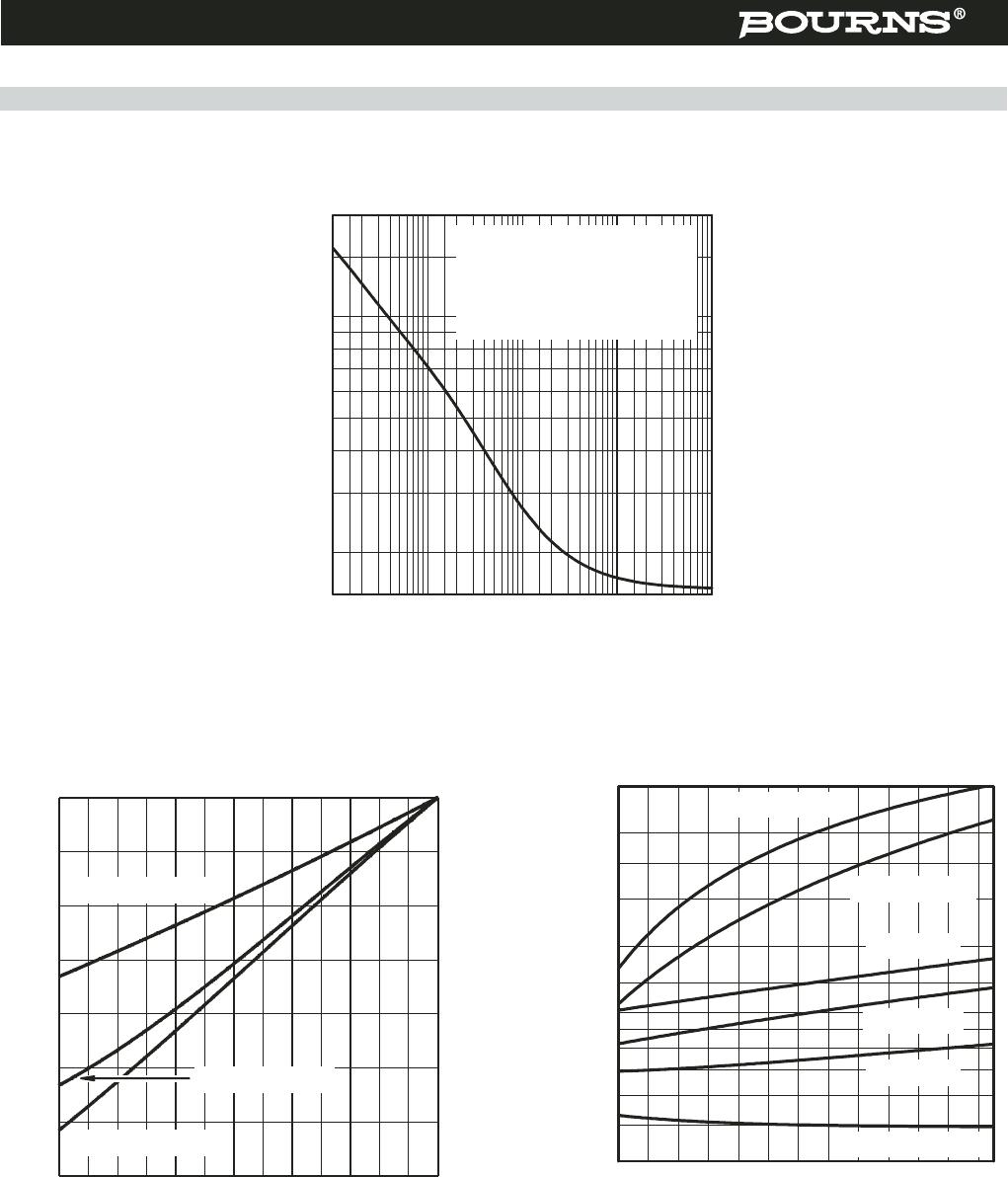
Figure 12. Two Point Protection
Th1
Figure 13. Multi-Point Protection
Th3
Th2
Th1
Standard
Peak Voltage
Setting
V
Voltage
Wave Shape
µs
Peak Current
Value
A
Current
Wave Shape
µs
TISP4XXXM3
25 °C Rating
A
Series
Resistance
Ω
GR-1089-CORE
2500 2/10 500 2/10 300
11
1000 10/1000 100 10/1000 50
FCC Part 68
(March 1998)
1500 10/160 200 10/160 120 2x5.6
800 10/560 100 10/560 75 3
1500 9/720 † 37.5 5/320 † 100 0
1000 9/720 † 25 5/320 † 100 0
I3124 1500 0.5/700 37.5 0.2/310 100 0
ITU-T K.20/K.21
1500
4000
10/700
37.5
100
5/310 100 0
† FCC Part 68 terminology for the waveforms produced by the ITU-T recommendation K.21 10/700 impulse generator