MC100E116FNG

© Semiconductor Components Industries, LLC, 2016
July, 2016 Rev. 11
1 Publication Order Number:
MC10E116/D
MC10E116, MC100E116
5 V ECL Quint Differential
Line Receiver
Description
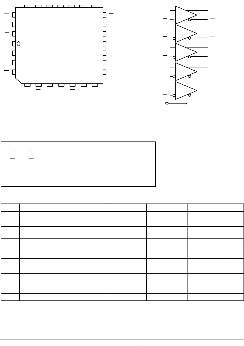
The MC10E/100E116 is a quint differential line receiver with
emitter-follower outputs. For applications which require bandwidths
greater than that of the E116, the E416 device may be of interest.
Active current sources plus a deep collector feature of the MOSAIC
III process provide the receivers with excellent common-mode noise
rejection. Each receiver has a dedicated V
CCO
supply lead, providing
optimum symmetry and stability.
If both inverting and non-inverting inputs are at an equal potential of
> 2.5 V, the receiver does not go to a defined state, but rather
current-shares in normal differential amplifier fashion, producing
output voltage levels midway between HIGH and LOW, or the device
may even oscillate.
The V
BB
pin, an internally generated voltage supply, is available to
this device only. For single-ended input conditions, the unused
differential input is connected to V
BB
as a switching reference voltage.
V
BB
may also rebias AC coupled inputs. When used, decouple V
BB
and V
CC
via a 0.01 mF capacitor and limit current sourcing or sinking
to 0.5 mA. When not used, V
BB
should be left open.
The 100 Series contains temperature compensation.
Features
500 ps Max. Propagation Delay
V
BB
Supply Output
Dedicated V
CCO
Pin for Each Receiver
PECL Mode Operating Range: V
CC
= 4.2 V to 5.7 V
with V
EE
= 0 V
NECL Mode Operating Range: V
CC
= 0 V
with V
EE
= 4.2 V to 5.7 V
Output Qs will default low when inputs are < V
CC
2.5 V
Internal Input 50 kW Pulldown Resistors
Meets or Exceeds JEDEC Spec EIA/JESD78 IC Latchup Test
ESD Protection:
> 2 kV Human Body Model
> 200 V Machine Model
Moisture Sensitivity: Level 3 (Pb-Free)
(For Additional Information, see Application Note AND8003/D
)
Flammability Rating: UL 94 V0 @ 0.125 in,
Oxygen Index: 28 to 34
Transistor Count = 98 Devices
These Devices are Pb-Free, Halogen Free and are RoHS Compliant
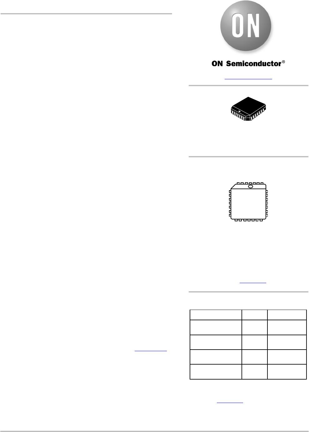
MARKING DIAGRAM*
xxx = 10 or 100
A = Assembly Location
WL = Wafer Lot
YY = Year
WW = Work Week
G = Pb-Free Package
PLCC28
FN SUFFIX
CASE 77602
MCxxxE116G
AWLYYWW
1
www.onsemi.com
*For additional marking information, refer to
Application Note AND8002/D
.
ORDERING INFORMATION
Device Package Shipping
MC10E116FNG PLCC28
(Pb-Free)
37 Units/Tube
MC10E116FNR2G
500 Tape & Reel
MC100E116FNR2G
MC100E116FNG
PLCC28
(Pb-Free)
PLCC28
(Pb-Free)
PLCC28
(Pb-Free)
37 Units/Tube
500 Tape & Reel
For information on tape and reel specifications, in-
cluding part orientation and tape sizes, please refer
to our Tape and Reel Packaging Specifications
Brochure, BRD8011/D
.
MC10E116, MC100E116
www.onsemi.com
2
V
CCO
D
1
D
3
Q
1
V
CCO
Q
0
Q
0
D
3
D
2
D
2
V
EE
V
BB
D
0
D
0
26
27
28
2
3
4
25 24 23 22 21 20 19
18
17
16
15
14
13
12
115678910
D
4
D
4
V
CCO
Q
4
Q
4
V
CCO
Q
3
Q
3
V
CC
Q
2
Q
2
V
CCO
Q
1
D
1
1
Pinout: 28-Lead PLCC
(Top View)
* All V
CC
and V
CCO
pins are tied together on the die.
Warning: All V
CC
, V
CCO
, and V
EE
pins must be externally
connected to Power Supply to guarantee proper operation.
Figure 1. Pinout Assignment Figure 2. Logic Diagram
D
0
D
0
D
1
D
1
D
2
D
2
D
3
D
3
D
4
D
4
V
BB
Q
0
Q
0
Q
1
Q
1
Q
2
Q
2
Q
3
Q
3
Q
4
Q
4
Table 1. PIN DESCRIPTION
PIN FUNCTION
D
0
, D
0
D
4
, D
4
ECL Differential Input Pairs
Q
0
, Q
0
Q
4
, Q
4
ECL Differential Output Pairs
V
BB
Reference Voltage Output.
V
CC
, V
CCO
Positive Supply
V
EE
Negative Supply
Table 2. MAXIMUM RATINGS
Symbol Parameter Condition 1 Condition 2 Rating Unit
V
CC
PECL Mode Power Supply V
EE
= 0 V 8 V
V
EE
NECL Mode Power Supply V
CC
= 0 V 6 V
V
I
PECL Mode Input Voltage
NECL Mode Input Voltage
V
EE
= 0 V
V
CC
= 0 V
V
I
V
CC
V
I
V
EE
6
6
V
I
out
Output Current Continuous
Surge
50
100
mA
I
BB
V
BB
Sink/Source ±0.5 mA
T
A
Operating Temperature Range 0 to +85 °C
T
stg
Storage Temperature Range 65 to +150 °C
q
JA
Thermal Resistance (Junction-to-Ambient) 0 lfpm
500 lfpm
PLCC28
PLCC28
63.5
43.5
°C/W
q
JC
Thermal Resistance (Junction-to-Case) Standard Board PLCC28 22 to 26 °C/W
T
sol
Wave Solder (Pb-Free) 265 °C
Stresses exceeding those listed in the Maximum Ratings table may damage the device. If any of these limits are exceeded, device functionality
should not be assumed, damage may occur and reliability may be affected.
MC10E116, MC100E116
www.onsemi.com
3
Table 3. 10E SERIES PECL DC CHARACTERISTICS (V
CCx
= 5.0 V, V
EE
= 0.0 V (Note 1))
Symbol
Characteristic
40°C 0°C 25°C 85°C
Unit
Min Typ Max Min Typ Max Min Typ Max Min Typ Max
I
EE
Power Supply Current 29 35 29 35 29 35 29 35 mA
V
OH
Output HIGH Voltage
(Note 2)
3980 4070 4160 4020 4105 4190 4090 4185 4280 mV
V
OL
Output LOW Voltage (Note 2) 3050 3210 3370 3050 3210 3370 3050 3227 3405 mV
V
IH
Input HIGH Voltage
(Single-Ended)
3830 3995 4160 3870 4030 4190 3940 4110 4280 mV
V
IL
Input LOW Voltage
(Single-Ended)
3050 3285 3520 3050 3285 3520 3050 3302 3555 mV
V
BB
Output Voltage Reference 3.57 3.7 3.57 3.7 3.65 3.75 3.69 3.81 V
V
IHCMR
Input HIGH Voltage Common
Mode Range (Differential
Configuration) (Note 3)
2.2 4.4 2.2 4.4 2.2 4.4 V
I
IH
Input HIGH Current 200 200 200 200
mA
I
IL
Input LOW Current 0.5 0.3 0.5 0.25 0.3 0.2
mA
NOTE: Device will meet the specifications after thermal equilibrium has been established when mounted in a test socket or printed circuit
board with maintained transverse airflow greater than 500 lfpm. Electrical parameters are guaranteed only over the declared
operating temperature range. Functional operation of the device exceeding these conditions is not implied. Device specification limit
values are applied individually under normal operating conditions and not valid simultaneously.
1. Input and output parameters vary 1:1 with V
CC
. V
EE
can vary 0.46 V / +0.06 V.
2. Outputs are terminated through a 50 W resistor to V
CC
2.0 V.
3. V
IHCMR
min varies 1:1 with V
EE
, max varies 1:1 with V
CC
.
Table 4. 10E SERIES NECL DC CHARACTERISTICS (V
CCx
= 0.0 V; V
EE
= 5.0 V (Note 1))
Symbol Characteristic
40°C 0°C 25°C 85°C
Unit
Min Typ Max Min Typ Max Min Typ Max Min Typ Max
I
EE
Power Supply Current 29 35 29 35 29 35 29 35 mA
V
OH
Output HIGH Voltage
(Note 2)
1020 930 840 980 895 810 910 815 720 mV
V
OL
Output LOW Voltage
(Note 2)
1950 1790 1630 1950 1790 1630 1950 1773 1595 mV
V
IH
Input HIGH Voltage
(Single-Ended)
1170 1005 840 1130 970 810 1060 890 720 mV
V
IL
Input LOW Voltage
(Single-Ended)
1950 1715 1480 1950 1715 1480 1950 1698 1445 mV
V
BB
Output Voltage Reference 1.43 1.3 1.13 1.30 1.35 1.25 1.31 1.19 V
V
IHCMR
Input HIGH Voltage
Common Mode Range
(Differential Configuration)
(Note 3)
2.8 0.6 2.8 0.6 2.8 0.6 V
I
IH
Input HIGH Current 200 200 200 200
mA
I
IL
Input LOW Current 0.5 0.3 0.5 0.065 0.3 0.2
mA
NOTE: Device will meet the specifications after thermal equilibrium has been established when mounted in a test socket or printed circuit
board with maintained transverse airflow greater than 500 lfpm. Electrical parameters are guaranteed only over the declared
operating temperature range. Functional operation of the device exceeding these conditions is not implied. Device specification limit
values are applied individually under normal operating conditions and not valid simultaneously.
1. Input and output parameters vary 1:1 with V
CC
. V
EE
can vary 0.46 V / +0.06 V.
2. Outputs are terminated through a 50 W resistor to V
CC
2.0 V.
3. V
IHCMR
min varies 1:1 with V
EE
, max varies 1:1 with V
CC
.

MC100E116FNG

Mfr. #:
Manufacturer:
ON Semiconductor
Description:
Bus Receivers 5V ECL Quint Diff Line Receiver
Lifecycle:
New from this manufacturer.
Delivery:
DHL FedEx Ups TNT EMS
Payment:
T/T Paypal Visa MoneyGram Western Union