MC100E116FNG

MC10E116, MC100E116
www.onsemi.com
4
Table 5. 100E SERIES PECL DC CHARACTERISTICS (V
CCx
= 5.0 V, V
EE
= 0.0 V (Note 1))
Symbol
Characteristic
40°C 0°C 25°C 85°C
Unit
Min Typ Max Min Typ Max Min Typ Max Min Typ Max
I
EE
Power Supply Current 29 35 29 35 29 35 29 35 mA
I
EE
Power Supply Current 29 35 29 35 29 35 29 40 mA
V
OH
Output HIGH Voltage
(Note 2)
3975 4050 4120 3975 4050 4120 3975 4050 4120 mV
V
OL
Output LOW Voltage
(Note 2)
3190 3295 3380 3190 3255 3380 3190 3260 3380 mV
V
IH
Input HIGH Voltage
(Single-Ended)
3975 3835 3975 4120 3835 3975 4120 3835 3975 4120 mV
V
IL
Input LOW Voltage
(Single-Ended)
3355 3190 3355 3525 3190 3355 3525 3190 3355 3525 mV
V
BB
Output Voltage Reference 3.62 3.74 3.64 3.75 3.62 3.74 3.62 3.74 V
V
IHCMR
Input HIGH Voltage Com-
mon Mode Range
(Differential Configuration)
(Note 3)
2.2 4.4 2.2 4.4 2.2 4.4 V
I
IH
Input HIGH Current 200 200 200 200
mA
I
IL
Input LOW Current 0.5 0.3 0.5 0.25 0.5 0.2
mA
NOTE: Device will meet the specifications after thermal equilibrium has been established when mounted in a test socket or printed circuit
board with maintained transverse airflow greater than 500 lfpm. Electrical parameters are guaranteed only over the declared
operating temperature range. Functional operation of the device exceeding these conditions is not implied. Device specification limit
values are applied individually under normal operating conditions and not valid simultaneously.
1. Input and output parameters vary 1:1 with V
CC
. V
EE
can vary 0.46 V / +0.8 V.
2. Outputs are terminated through a 50 W resistor to V
CC
2.0 V.
3. V
IHCMR
min varies 1:1 with V
EE
, max varies 1:1 with V
CC
.
MC10E116, MC100E116
www.onsemi.com
5
Table 6. 100E SERIES NECL DC CHARACTERISTICS (V
CCx
= 0.0 V; V
EE
= 5.0 V (Note 1))
Symbol Characteristic
40°C 0°C 25°C 85°C
Unit
Min Typ Max Min Typ Max Min Typ Max Min Typ Max
I
EE
Power Supply
Current
29 35 29 35 29 35 29 40 mA
V
OH
Output HIGH Voltage
(Note 2)
1025 950 880 1025 950 880 1025 950 880 mV
V
OL
Output LOW Voltage
(Note 2)
1810 1705 1620 1810 1745 1620 1810 1740 1620 mV
V
IH
Input HIGH Voltage
(Single-Ended)
1025 1165 1025 880 1165 1025 880 1165 1025 880 mV
V
IL
Input LOW Voltage
(Single-Ended)
1645 1810 1645 1475 1810 1645 1475 1810 1645 1475 mV
V
BB
Output Voltage
Reference
1.38 1.26 1.38 1.25 1.38 1.26 1.38 1.26 V
V
IHCMR
Input HIGH Voltage
Common Mode
Range (Differential
Configuration)
(Note 3)
2.8 0.6 2.8 0.6 2.8 0.6 V
I
IH
Input HIGH Current 200 200 200 200
mA
I
IL
Input LOW Current 0.5 0.3 0.5 0.25 0.5 0.2
mA
NOTE: Device will meet the specifications after thermal equilibrium has been established when mounted in a test socket or printed circuit
board with maintained transverse airflow greater than 500 lfpm. Electrical parameters are guaranteed only over the declared
operating temperature range. Functional operation of the device exceeding these conditions is not implied. Device specification limit
values are applied individually under normal operating conditions and not valid simultaneously.
1. Input and output parameters vary 1:1 with V
CC
. V
EE
can vary 0.46 V / +0.8 V.
2. Outputs are terminated through a 50 W resistor to V
CC
2.0 V.
3. V
IHCMR
min varies 1:1 with V
EE
, max varies 1:1 with V
CC
.
MC10E116, MC100E116
www.onsemi.com
6
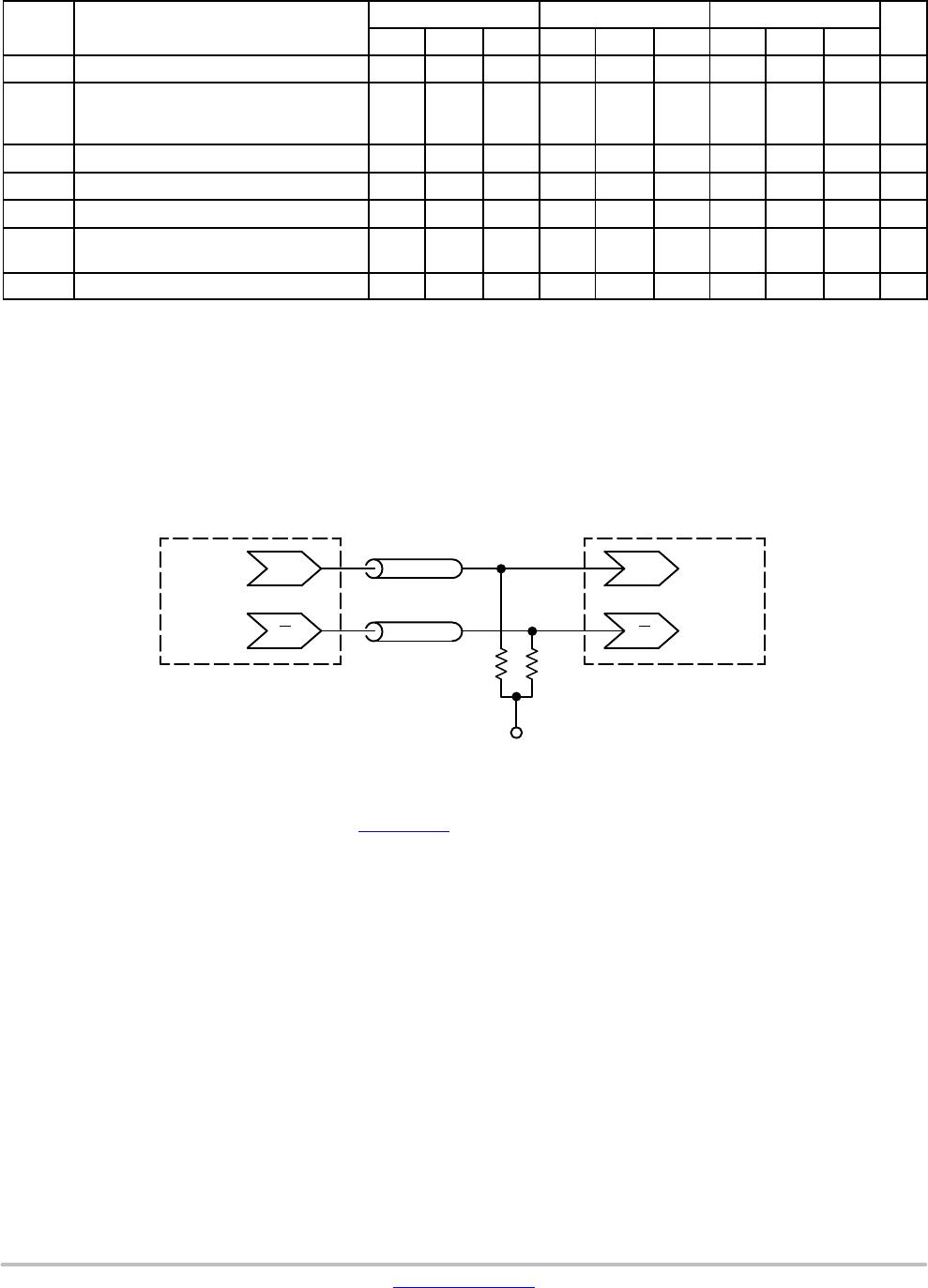
Table 7. AC CHARACTERISTICS (V
CCx
= 5.0 V; V
EE
= 0.0 V or V
CCx
= 0.0 V; V
EE
= 5.0 V (Note 1))
Symbol
Characteristic
40°C 25°C 85°C
Unit
Min Typ Max Min Typ Max Min Typ Max
f
MAX
Maximum Toggle Frequency 800 800 800 MHz
t
PLH
t
PHL
Propagation Delay to Output
D (Differential Configuration)
D (Single-Ended)
150
150
300
300
500
550
200
150
300
300
450
500
200
150
300
300
450
500
ps
t
skew
Within-Device Skew (Note 2) 50 50 50 ps
t
skew
Duty Cycle Skew (Note 3) t
PLH
t
PHL
±10 ±10 ±10 ps
t
JITTER
Random Clock Jitter (RMS) < 1 < 1 < 1 ps
V
PP
Input Voltage Swing
(Differential Configuration)
150 150 150 mV
t
r
/t
f
Rise/Fall Time 2080% 250 375 625 275 375 575 275 375 575 ps
NOTE: Device will meet the specifications after thermal equilibrium has been established when mounted in a test socket or printed circuit
board with maintained transverse airflow greater than 500 lfpm. Electrical parameters are guaranteed only over the declared
operating temperature range. Functional operation of the device exceeding these conditions is not implied. Device specification limit
values are applied individually under normal operating conditions and not valid simultaneously.
1. 10 Series: V
EE
can vary 0.46 V / +0.06 V.
100 Series: V
EE
can vary 0.46 V / +0.8 V.
2. Within-device skew is defined as identical transitions on similar paths through a device.
3. Duty cycle skew is defined only for differential operation when the delays are measured from the cross point of the inputs to the cross point
of the outputs.
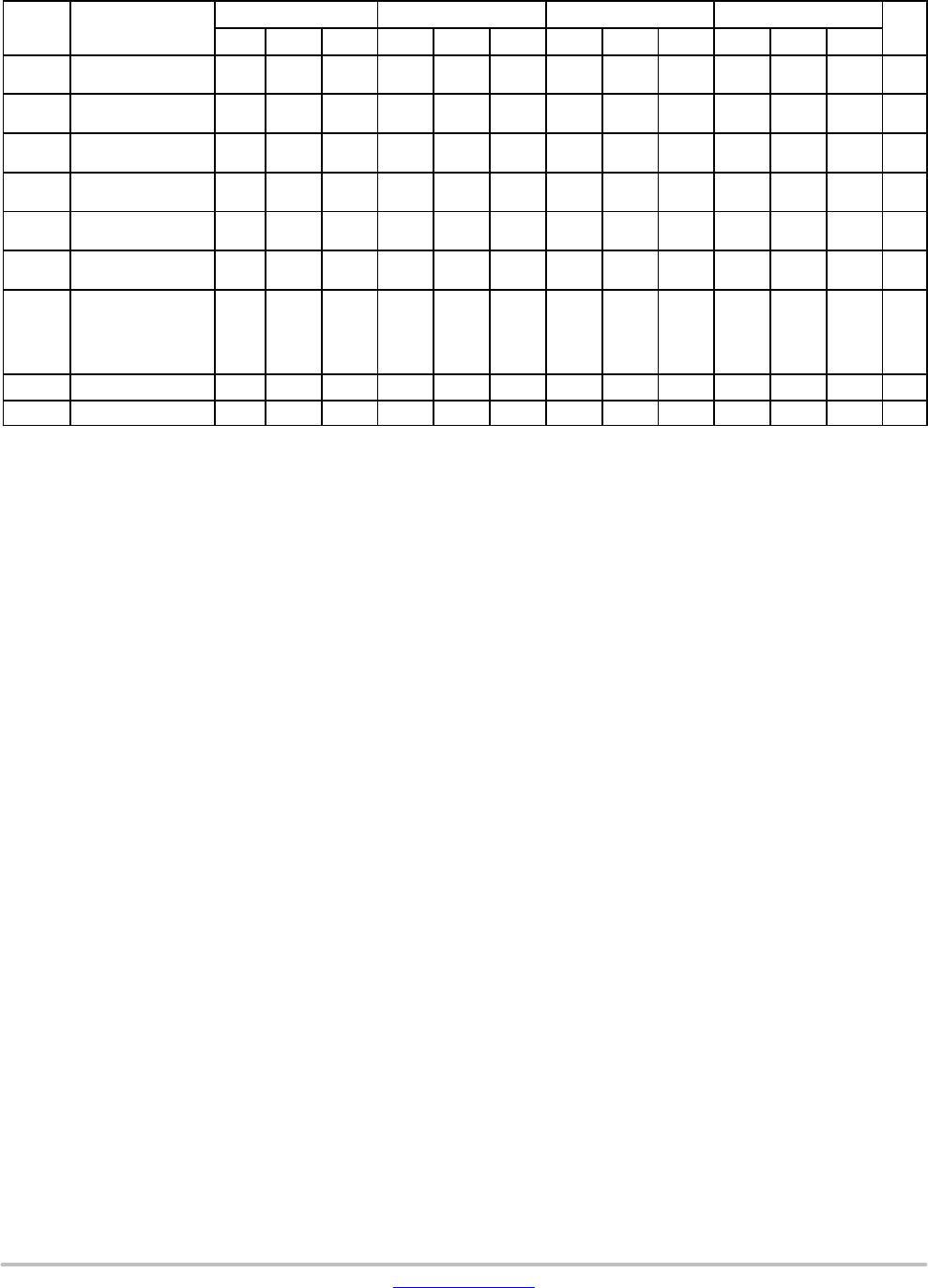
Figure 3. Typical Termination for Output Driver and Device Evaluation
(See Application Note AND8020/D
Termination of ECL Logic Devices)
Driver
Device
Receiver
Device
QD
Q D
Z
o
= 50 W
Z
o
= 50 W
50 W 50 W
V
TT
V
TT
= V
CC
2.0 V
Resource Reference of Application Notes
AN1405/D ECL Clock Distribution Techniques
AN1406/D Designing with PECL (ECL at +5.0 V)
AN1503/D
ECLinPSt I/O SPiCE Modeling Kit
AN1504/D Metastability and the ECLinPS Family
AN1568/D Interfacing Between LVDS and ECL
AN1672/D The ECL Translator Guide
AND8001/D Odd Number Counters Design
AND8002/D Marking and Date Codes
AND8020/D Termination of ECL Logic Devices
AND8066/D Interfacing with ECLinPS
AND8090/D AC Characteristics of ECL Devices

MC100E116FNG

Mfr. #:
Manufacturer:
ON Semiconductor
Description:
Bus Receivers 5V ECL Quint Diff Line Receiver
Lifecycle:
New from this manufacturer.
Delivery:
DHL FedEx Ups TNT EMS
Payment:
T/T Paypal Visa MoneyGram Western Union