3
LT1225
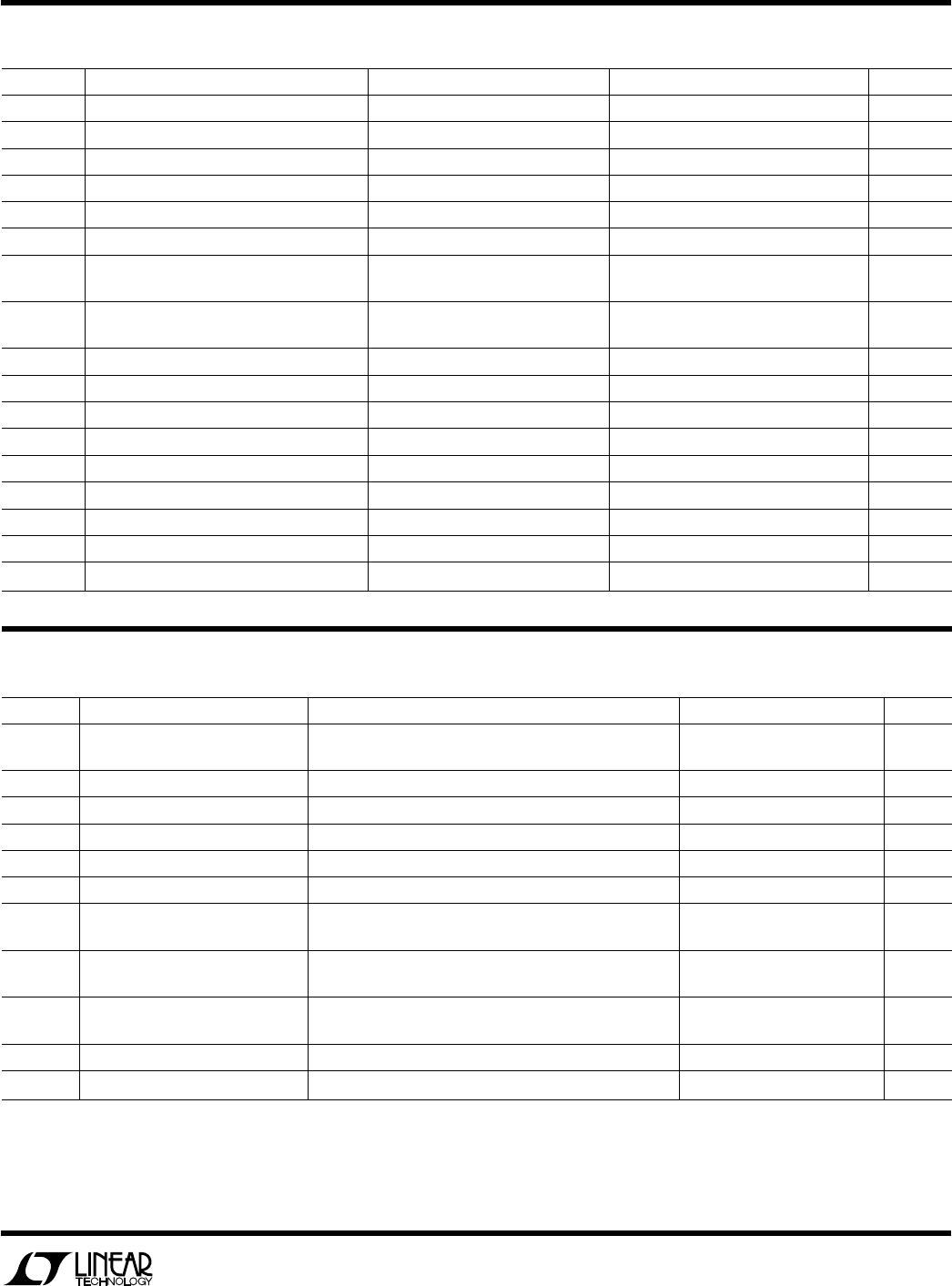
SYMBOL PARAMETER CONDITIONS MIN TYP MAX UNITS
V
OS
Input Offset Voltage V
S
= ±15V, (Note 2) 0.5 1.5 mV
V
S
= ±5V, (Note 2) 1.0 2.5 mV
Input V
OS
Drift 10 µV/°C
I
OS
Input Offset Current V
S
= ±15V and V
S
= ±5V 100 600 nA
I
B
Input Bias Current V
S
= ±15V and V
S
= ±5V 4 9 µA
CMRR Common-Mode Rejection Ratio V
S
= ±15V, V
CM
= ±12V and V
S
= ±5V, V
CM
= ±2.5V 93 115 dB
PSRR Power Supply Rejection Ratio V
S
= ±5V to ±15V 85 95 dB
A
VOL
Large Signal Voltage Gain V
S
= ±15V, V
OUT
= ±10V, R
L
= 500Ω 10 12.5 V/mV
V
S
= ±5V, V
OUT
= ±2.5V, R
L
= 500Ω 8 10 V/mV
V
OUT
Output Swing V
S
= ±15V, R
L
= 500Ω±12.0 ±13.3 V
V
S
= ±5V, R
L
= 500Ω or 150Ω ±3.0 ±3.3 V
I
OUT
Output Current V
S
= ±15V, V
OUT
= ±12V 24 40 mA
V
S
= ±5V, V
OUT
= ±3V 20 40 mA
SR Slew Rate V
S
= ±15V, (Note 3) 250 400 V/µs
I
S
Supply Current V
S
= ±15V and V
S
= ±5V 7 10.5 mA
V
S
= ±5V, T
A
= 25°C, V
CM
= 0V unless otherwise noted.
SYMBOL PARAMETER CONDITIONS MIN TYP MAX UNITS
V
OS
Input Offset Voltage (Note 2) 1.0 2.0 mV
I
OS
Input Offset Current 100 400 nA
I
B
Input Bias Current 48 µA
Input Voltage Range + 2.5 4 V
Input Voltage Range – –3 –2.5 V
CMRR Common-Mode Rejection Ratio V
CM
= ±2.5V 94 115 dB
A
VOL
Large-Signal Voltage Gain V
OUT
= ±2.5V, R
L
= 500Ω 10 15 V/mV
V
OUT
= ±2.5V, R
L
= 150Ω 13 V/mV
V
OUT
Output Voltage R
L
= 500Ω±3.0 ±3.7 V
R
L
= 150Ω±3.0 ±3.3 V
I
OUT
Output Current V
OUT
= ±3V 20 40 mA
SR Slew Rate (Note 3) 250 V/µs
Full Power Bandwidth 3V Peak, (Note 4) 13.3 MHz
GBW Gain Bandwidth f = 1MHz 100 MHz
t
r
, t
f
Rise Time, Fall Time A
VCL
= 5, 10% to 90%, 0.1V 9 ns
Overshoot A
VCL
= 5, 0.1V 10 %
Propagation Delay 50% V
IN
to 50% V
OUT
9ns
t
s
Settling Time – 2.5V to 2.5V, 0.1%, A
V
= –4 70 ns
I
S
Supply Current 79 mA
E
LECTR
IC
AL C CHARA TERIST
ICS
E
LECTR
IC
AL C CHARA TERIST
ICS
Note 3: Slew rate is measured between ±10V on an output swing of ±12V
on ±15V supplies, and ±2V on an output swing of ±3.5V on ±5V supplies.
Note 4: Full power bandwidth is calculated from the slew rate
measurement: FPBW = SR/2πVp.
Note 1: A heat sink may be required to keep the junction temperature
below absolute maximum when the output is shorted indefinitely.
Note 2: Input offset voltage is tested with automated test equipment
in <1 second.
0°C ≤ T
A
≤ 70°C, V
CM
= 0V unless otherwise noted.