LT1225CN8#PBF

LT1225
4
CCHARA TERIST
ICS
UW
AT
Y
P
I
CA
LPER
F
O
R
C
E
Output Short-Circuit Current vs
Supply Current vs Temperature Input Bias Current vs Temperature Temperature
Output Voltage Swing vs Input Bias Current vs Input Open-Loop Gain vs
Resistive Load Common-Mode Voltage Resistive Load
Input Common-Mode Range vs Output Voltage Swing vs
Supply Voltage Supply Current vs Supply Voltage Supply Voltage
SUPPLY VOLTAGE (±V)
0
0
MAGNITUDE OF INPUT VOLTAGE (V)
5
10
15
20
5101520
LT1225 TPC01
T
A
= 25°C
V
OS
< 1mV
+V
CM
–V
CM
SUPPLY VOLTAGE (±V)
0
6.0
SUPPLY CURRENT (mA)
6.5
7.0
7.5
8.0
5101520
LT1225 TPC02
T
A
= 25°C
SUPPLY VOLTAGE (±V)
0
0
OUTPUT VOLTAGE SWING (V)
5
10
15
20
5101520
LT1225 TPC03
T
A
= 25°C
R
L
= 500
V
OS
= 30mV
+V
SW
–V
SW
LOAD RESISTANCE ()
10
0
OUTPUT VOLTAGE SWING (Vp-p)
10
20
25
30
100 1k 10k
LT1225 TPC04
15
5
T
A
= 25°C
V
OS
= 30mV
V
S
= ±15V
V
S
= ±5V
INPUT COMMON-MODE VOLTAGE (V)
–15
3.0
INPUT BIAS CURRENT (µA)
3.5
4.0
4.5
5.0
–10 0 10 15
LT1225 TPC05
–5 5
V
S
= ±15V
T
A
= 25°C
I
B+
+ I
B–
2
I
B
=
LOAD RESISTANCE ()
10
50
OPEN-LOOP GAIN (dB)
80
90
100
100 1k 10k
LT1225 TPC06
70
60
T
A
= 25°C
V
S
= ±15V
V
S
= ±5V
TEMPERATURE (°C)
–50
25
OUTPUT SHORT-CIRCUIT CURRENT (mA)
35
40
50
55
–25 25 75 125
LT1225 TPC09
100500
30
45
V
S
= ±5V
SINK
SOURCE
TEMPERATURE (°C)
–50
3.5
INPUT BIAS CURRENT (µA)
4.0
4.25
4.75
5.0
–25 25 75 125
LT1225 TPC08
100500
3.75
4.5
V
S
= ±15V
I
B+
+ I
B–
2
I
B
=
TEMPERATURE (°C)
–50
4
SUPPLY CURRENT (mA)
6
7
9
10
–25 25 75 125
LT1225 TPC07
V
S
= ±15V
100500
5
8
5
LT1225
CCHARA TERIST
ICS
UW
AT
Y
P
I
CA
LPER
F
O
R
C
E
Closed-Loop Output Impedance vs
Frequency Gain Bandwidth vs Temperature Slew Rate vs Temperature
Power Supply Rejection Ratio vs Common-Mode Rejection Ratio vs
Input Noise Spectral Density Frequency Frequency
TEMPERATURE (˚C)
–50
GAIN BANDWIDTH (MHz)
151
152
153
25 75
LT1225 TPC17
150
149
–25 0
50 100 125
148
147
V
S
= ±15V
TEMPERATURE (˚C)
–50
SLEW RATE (V/µs)
400
450
500
25 75
LT1225 TPC18
350
300
–25 0
50 100 125
250
200
–SR
+SR
V
S
= ±15V
A
V
= –5
FREQUENCY (Hz)
INPUT VOLTAGE NOISE (nV/Hz)
1
100
10 1k 10k 100k
LT1225 TPC10
100
1000
10
V
S
= ±15V
T
A
= 25°C
A
V
= 101
R
S
= 100k
i
n
e
n
0.01
1.0
10
0.1
INPUT CURRENT NOISE (pA/Hz)
FREQUENCY (Hz)
100
0
POWER SUPPLY REJECTION RATIO (dB)
20
40
60
80
100
1k
10k 100k 1M
LT1225 TPC11
10M 100M
V
S
= ±15V
T
A
= 25°C
+PSRR
PSRR
Voltage Gain and Phase vs Frequency Response vs
Frequency Output Swing vs Settling Time Capacitive Load
SETTLING TIME (ns)
0
OUTPUT SWING (V)
2
6
10
80
–2
–6
–10
20
40
60
100
120
LTC1225 TPC14
0
4
8
–4
–8
V
S
= ±15
T
A
= 25°C
10mV SETTLING
A
V
= 5
A
V
= –5
A
V
= –5
A
V
= 5
FREQUENCY (HZ)
1M
4
VOLTAGE MAGNITUDE (dB)
8
12
16
20
24
10M 100M
V
S
= ±15V
T
A
= 25°C
A
V
= –5
C = 100pF
C = 0pF
C = 50pF
LT1225 TPC15
6
10
14
18
22
C = 1000pF 
C = 500pF
FREQUENCY (Hz)
10k
OUTPUT IMPEDANCE ()
1
10
100M
LT1225 TPC16
0.1
0.01
100k
1M
10M
100
V
S
= ±15V
T
A
= 25°C
A
V
= 5
FREQUENCY (Hz)
100
0
VOLTAGE GAIN (dB)
20
40
60
80
100
1k
10k 100k 1M
LT1225 TPC13
10M 100M
0
20
40
60
80
100
PHASE MARGIN (DEG)
V
S
= ±15V
V
S
= ±5V
T
A
= 25°C
V
S
= ±5V
V
S
= ±15V
LT1225
6
Small Signal, A
V
= 5 Small Signal, A
V
= –5
U
S
A
O
PP
L
IC
AT
I
WU
U
I FOR ATIO
The LT1225 may be inserted directly into HA2541, HA2544,
AD847, EL2020 and LM6361 applications, provided that
the amplifier configuration is a noise gain of 5 or greater,
and the nulling circuitry is removed. The suggested nulling
circuit for the LT1225 is shown below.
Offset Nulling
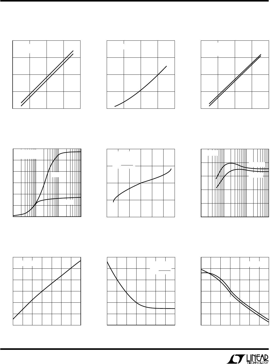
The large-signal response in both inverting and noninvert-
ing gain shows symmetrical slewing characteristics. Nor-
mally the noninverting response has a much faster rising
edge than falling edge due to the rapid change in input
common-mode voltage which affects the tail current of the
input differential pair. Slew enhancement circuitry has
been added to the LT1225 so that the noninverting slew
rate response is balanced.
Large Signal, A
V
= 5 Large Signal, A
V
= –5
Input Considerations
Resistors in series with the inputs are recommended for
the LT1225 in applications where the differential input
voltage exceeds ±6V continuously or on a transient basis.
An example would be in noninverting configurations with
high input slew rates or when driving heavy capacitive
loads. The use of balanced source resistance at each input
is recommended for applications where DC accuracy must
be maximized.
Capacitive Loading
The LT1225 is stable with all capacitive loads. This is
accomplished by sensing the load induced output pole and
adding compensation at the amplifier gain node. As the
capacitive load increases, both the bandwidth and phase
margin decrease so there will be peaking in the frequency
Layout and Passive Components
As with any high speed operational amplifier, care must be
taken in board layout in order to obtain maximum perfor-
mance. Key layout issues include: use of a ground plane,
minimization of stray capacitance at the input pins, short
lead lengths, RF-quality bypass capacitors located close
to the device (typically 0.01µF to 0.1µF), and use of low
ESR bypass capacitors for high drive current applications
(typically 1µF to 10µF tantalum). Sockets should be
avoided when maximum frequency performance is
required, although low profile sockets can provide
reasonable performance up to 50MHz. For more details
see Design Note 50. Feedback resistor values greater than
5k are not recommended because a pole is formed with the
input capacitance which can cause peaking. If feedback
resistors greater than 5k are used, a parallel
capacitor of 5pF to 10pF should be used to cancel the input
pole and optimize dynamic performance.
Transient Response
The LT1225 gain-bandwidth is 150MHz when measured at
1MHz. The actual frequency response in gain of 5 is
considerably higher than 30MHz due to peaking caused by
a second pole beyond the gain of 5 crossover point. This
is reflected in the small-signal transient response. Higher
noise gain configurations exhibit less overshoot as seen in
the inverting gain of 5 response.
+
3
2
1
8
5k
0.1µF
7
6
4
0.1µF
V
+
V
LT1225
LT1225 AI01
LT1225 AI02
LT1225 AI03

LT1225CN8#PBF

Mfr. #:
Manufacturer:
Analog Devices Inc.
Description:
High Speed Operational Amplifiers Very Hi Speed Op Amp
Lifecycle:
New from this manufacturer.
Delivery:
DHL FedEx Ups TNT EMS
Payment:
T/T Paypal Visa MoneyGram Western Union

Products related to this Datasheet