74HC4050_Q100 All information provided in this document is subject to legal disclaimers. © NXP B.V. 2013. All rights reserved.
Product data sheet Rev. 1 — 30 January 2013 3 of 13
NXP Semiconductors
74HC4050-Q100
Hex non-inverting HIGH-to-LOW level shifter
5.2 Pin description
6. Functional description
[1] H = HIGH voltage level; L = LOW voltage level; X = don’t care; Z = high-impedance OFF-state.
7. Limiting values
[1] For SO16 packages: P
tot
derates linearly with 8 mW/K above 70 C.
For TSSOP16 packages: P
tot
derates linearly with 5.5 mW/K above 60 C.
Table 2. Pin description
Symbol Pin Description
V
CC
1 supply voltage
1Y to 6Y 2, 4, 6, 10, 12, 15 output
1A to 6A 3, 5, 7, 9, 11, 14 input
GND 8 ground (0 V)
n.c. 13, 16 not connected
Table 3. Function table
[1]
Input Output
nA nY
LL
HH
Table 4. Limiting values
In accordance with the Absolute Maximum Rating System (IEC 60134). Voltages are referenced to GND (ground = 0 V).
Symbol Parameter Conditions Min Max Unit
V
CC
supply voltage 0.5 +7 V
V
IK
input clamping voltage 0.5 +16 V
I
IK
input clamping current V
I
< 0.5 V 20 - mA
I
OK
output clamping current V
O
< 0.5 V or V
O
>V
CC
+0.5V - 20 mA
I
O
output current V
O
= 0.5 V to (V
CC
+0.5V) - 25 mA
I
CC
supply current - +50 mA
I
GND
ground current - 50 mA
T
stg
storage temperature 65 +150 C
P
tot
total power dissipation
[1]
- 500 mW
74HC4050_Q100 All information provided in this document is subject to legal disclaimers. © NXP B.V. 2013. All rights reserved.
Product data sheet Rev. 1 — 30 January 2013 4 of 13
NXP Semiconductors
74HC4050-Q100
Hex non-inverting HIGH-to-LOW level shifter
8. Recommended operating conditions
9. Static characteristics
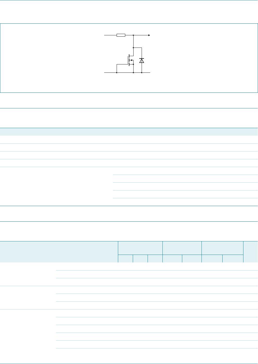
Fig 6. Input protection for the 74HC4050-Q100
001aan375
100 Ω
D1
polysilicon
resistor
to logic
circuit
input
GND
Table 5. Recommended operating conditions
Voltages are referenced to GND (ground = 0 V)
Symbol Parameter Conditions Min Typ Max Unit
V
CC
supply voltage 2.0 5.0 6.0 V
V
I
input voltage 0 - 15 V
V
O
output voltage 0 - V
CC
V
T
amb
ambient temperature 40 +25 +125 C
t/V input transition rise and fall rate V
CC
= 2.0 V; V
I
= 2.0 V - - 625 ns/V
V
CC
= 4.5 V; V
I
= 4.5 V - 1.67 139 ns/V
V
CC
= 6.0 V; V
I
= 6.0 V - - 83 ns/V
V
CC
= 6.0 V; V
I
= 10.0 V - - 81 ns/V
V
CC
= 6.0 V; V
I
= 15.0 V - - 83 ns/V
Table 6. Static characteristics
At recommended operating conditions; voltages are referenced to GND (ground = 0 V).
Symbol Parameter Conditions T
amb
= 25 C T
amb
= 40 C to
+85 C
T
amb
= 40 C to
+125 C
Unit
Min Typ Max Min Max Min Max
V
IH
HIGH-level
input voltage
V
CC
= 2.0 V 1.5 1.3 - 1.5 - 1.5 - V
V
CC
= 4.5 V 3.15 2.4 - 3.15 - 3.15 - V
V
CC
= 6.0 V 4.2 3.1 - 4.2 - 4.2 - V
V
IL
LOW-level
input voltage
V
CC
= 2.0 V - 0.7 0.5 - 0.5 - 0.5 V
V
CC
= 4.5 V - 1.8 1.35 - 1.35 - 1.35 V
V
CC
= 6.0 V - 2.3 1.8 - 1.8 - 1.8 V
V
OH
HIGH-level
output voltage
V
I
=V
IH
or V
IL
I
O
= 20 A; V
CC
= 2.0 V 1.9 2.0 - 1.9 - 1.9 - V
I
O
= 20 A; V
CC
= 4.5 V 4.4 4.5 - 4.4 - 4.4 - V
I
O
= 20 A; V
CC
= 6.0 V 5.9 6.0 - 5.9 - 5.9 - V
I
O
= 4.0 mA; V
CC
= 4.5 V 3.98 - - 3.84 - 3.7 - V
I
O
= 5.2 mA; V
CC
= 6.0 V 5.48 - - 5.34 - 5.2 - V
74HC4050_Q100 All information provided in this document is subject to legal disclaimers. © NXP B.V. 2013. All rights reserved.
Product data sheet Rev. 1 — 30 January 2013 5 of 13
NXP Semiconductors
74HC4050-Q100
Hex non-inverting HIGH-to-LOW level shifter
10. Dynamic characteristics
V
OL
LOW-level
output voltage
V
I
=V
IH
or V
IL
I
O
=20A; V
CC
= 2.0 V - - 0.1 - 0.1 - 0.1 V
I
O
=20A; V
CC
= 4.5 V - - 0.1 - 0.1 - 0.1 V
I
O
=20A; V
CC
= 6.0 V - - 0.1 - 0.1 - 0.1 V
I
O
= 4.0 mA; V
CC
= 4.5 V - - 0.26 - 0.33 - 0.4 V
I
O
= 5.2 mA; V
CC
= 6.0 V - - 0.26 - 0.33 - 0.4 V
I
I
input leakage
current
V
I
=V
CC
or GND;
V
CC
=6.0V
--0.1 - 1.0 - 1.0 A
V
I
= 15 V; V
CC
= 2.0 V to
6.0 V
--0.5 - 5.0 - 5.0 A
I
CC
supply current V
I
= 15 V or GND; I
O
=0A;
V
CC
=6.0V
--2.0- 20 - 40A
C
I
input
capacitance
-3.5- - - - -pF
Table 6. Static characteristics
…continued
At recommended operating conditions; voltages are referenced to GND (ground = 0 V).
Symbol Parameter Conditions T
amb
= 25 C T
amb
= 40 C to
+85 C
T
amb
= 40 C to
+125 C
Unit
Min Typ Max Min Max Min Max
Table 7. Dynamic characteristics
Voltages are referenced to GND (ground = 0 V); C
L
= 50 pF unless otherwise specified; for test circuit see Figure 8.
Symbol Parameter Conditions T
amb
= 25 C T
amb
= 40 C
to +85 C
T
amb
= 40 C
to +125 C
Unit
Min Typ Max Min Max Min Max
t
pd
propagation
delay
nA to nY; see Figure 7
[1]
V
CC
= 2.0 V - 25 85 - 105 - 130 ns
V
CC
= 4.5 V - 9 17 - 21 - 26 ns
V
CC
=5V; C
L
=15pF - 7 - - - - - ns
V
CC
= 6.0 V - 7 14 - 18 - 22 ns
t
t
transition
time
Yn; see Figure 7
[2]
V
CC
= 2.0 V - 19 75 - 95 - 110 ns
V
CC
= 4.5 V - 7 15 - 19 - 22 ns
V
CC
= 6.0 V - 6 13 - 16 - 19 ns

74HC4050D-Q100J

Mfr. #:
Manufacturer:
Nexperia
Description:
Buffers & Line Drivers 74HC4050D-Q100/SO16/REEL 13" Q
Lifecycle:
New from this manufacturer.
Delivery:
DHL FedEx Ups TNT EMS
Payment:
T/T Paypal Visa MoneyGram Western Union

Products related to this Datasheet