74HC4050_Q100 All information provided in this document is subject to legal disclaimers. © NXP B.V. 2013. All rights reserved.
Product data sheet Rev. 1 — 30 January 2013 6 of 13
NXP Semiconductors
74HC4050-Q100
Hex non-inverting HIGH-to-LOW level shifter
[1] t
pd
is the same as t
PLH
and t
PHL
.
[2] t
t
is the same as t
THL
and t
TLH
.
[3] C
PD
is used to determine the dynamic power dissipation (P
D
in W).
P
D
=C
PD
V
CC
2
f
i
N+(C
L
V
CC
2
f
o
) where:
f
i
= input frequency in MHz;
f
o
= output frequency in MHz;
C
L
= output load capacitance in pF;
V
CC
= supply voltage in V;
N = number of inputs switching;
(C
L
V
CC
2
f
o
) = sum of outputs.
11. Waveforms
C
PD
power
dissipation
capacitance
C
L
=50pF;f=1 MHz;
V
I
=GNDtoV
CC
[3]
-14- - - - -pF
Table 7. Dynamic characteristics
…continued
Voltages are referenced to GND (ground = 0 V); C
L
= 50 pF unless otherwise specified; for test circuit see Figure 8.
Symbol Parameter Conditions T
amb
= 25 C T
amb
= 40 C
to +85 C
T
amb
= 40 C
to +125 C
Unit
Min Typ Max Min Max Min Max
Measurement points are given in Table 8.
V
OL
and V
OH
are typical voltage output levels that occur with the output load.
Fig 7. The input (nA) to output (nY) propagation delays
DDD
W
3/+
W
3+/
9
0
9
0


9
0
9
0
Q<
RXWSXW
Q
$LQSXW
9
,
*1'
9
2+
9
2/
W
7/+
W
7+/
Table 8. Measurement points
Type Input Output
V
M
V
M
74HC4050-Q100 0.5V
CC
0.5V
CC
74HC4050_Q100 All information provided in this document is subject to legal disclaimers. © NXP B.V. 2013. All rights reserved.
Product data sheet Rev. 1 — 30 January 2013 7 of 13
NXP Semiconductors
74HC4050-Q100
Hex non-inverting HIGH-to-LOW level shifter
Test data is given in Table 9.
Definitions test circuit:
R
T
= Termination resistance should be equal to output impedance Z
o
of the pulse generator.
C
L
= Load capacitance including jig and probe capacitance.
R
L
= Load resistance.
S1 = Test selection switch.
Fig 8. Test circuit for measuring switching times
001aah768
t
W
t
W
t
r
t
r
t
f
V
M
V
I
negative
pulse
GND
V
I
positive
pulse
GND
10 %
90 %
90 %
10 %
V
M
V
M
V
M
t
f
V
CC
DUT
R
T
V
I
V
O
C
L
G
Table 9. Test data
Type Input Load Test
V
I
t
r
, t
f
C
L
74HC4050-Q100 V
CC
6.0 ns 15 pF, 50 pF t
PLH
, t
PHL
74HC4050_Q100 All information provided in this document is subject to legal disclaimers. © NXP B.V. 2013. All rights reserved.
Product data sheet Rev. 1 — 30 January 2013 8 of 13
NXP Semiconductors
74HC4050-Q100
Hex non-inverting HIGH-to-LOW level shifter
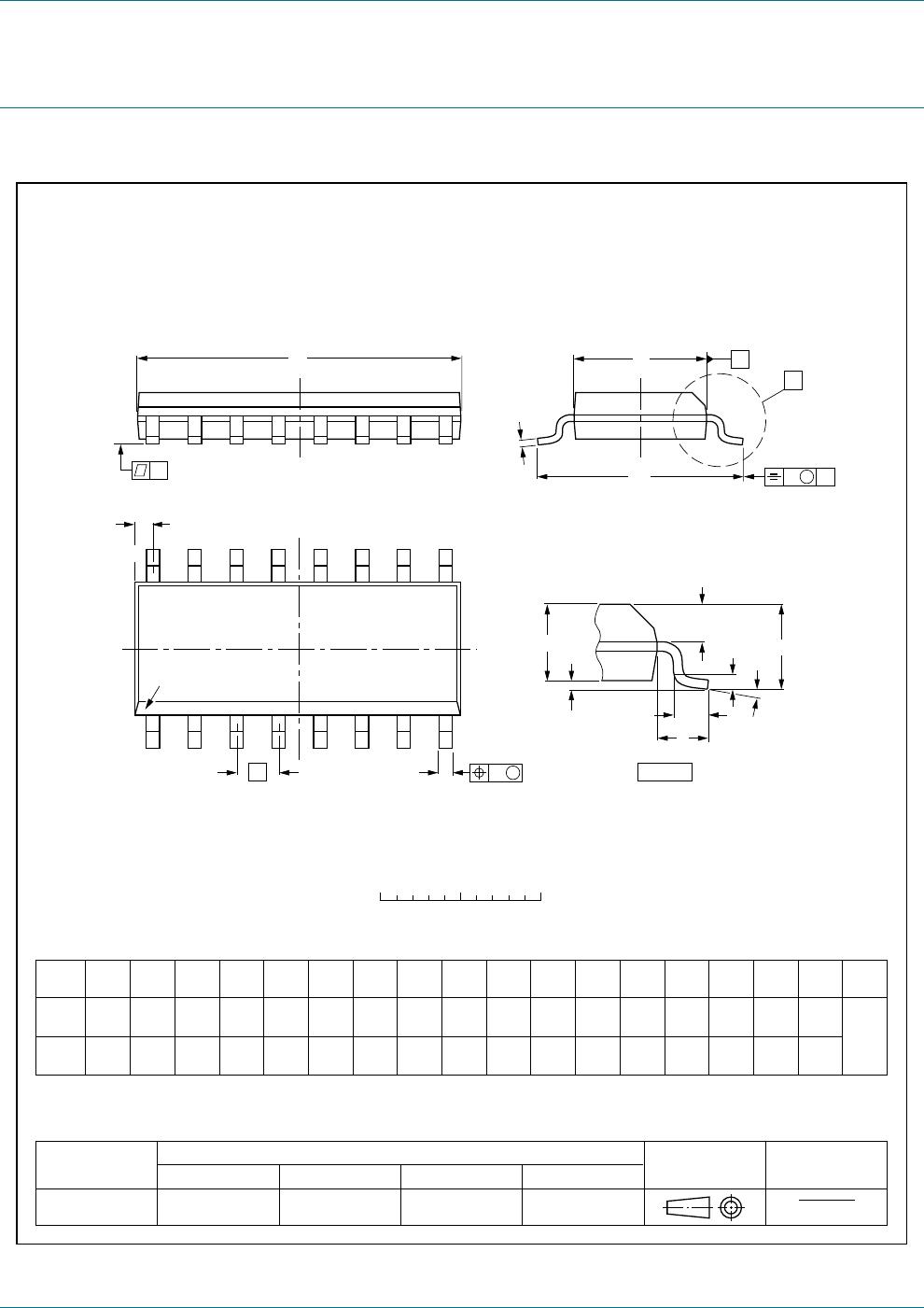
12. Package outline
Fig 9. Package outline SOT109-1 (SO16)
X
w M
θ
A
A
1
A
2
b
p
D
H
E
L
p
Q
detail X
E
Z
e
c
L
v M
A
(A )
3
A
8
9
1
16
y
pin 1 index
UNIT
A
max.
A
1
A
2
A
3
b
p
cD
(1)
E
(1) (1)
eH
E
LL
p
QZywv θ
REFERENCES
OUTLINE
VERSION
EUROPEAN
PROJECTION
ISSUE DATE
IEC JEDEC JEITA
mm
inches
1.75
0.25
0.10
1.45
1.25
0.25
0.49
0.36
0.25
0.19
10.0
9.8
4.0
3.8
1.27
6.2
5.8
0.7
0.6
0.7
0.3
8
0
o
o
0.25 0.1
DIMENSIONS (inch dimensions are derived from the original mm dimensions)
Note
1. Plastic or metal protrusions of 0.15 mm (0.006 inch) maximum per side are not included.
1.0
0.4
SOT109-1
99-12-27
03-02-19
076E07 MS-012
0.069
0.010
0.004
0.057
0.049
0.01
0.019
0.014
0.0100
0.0075
0.39
0.38
0.16
0.15
0.05
1.05
0.041
0.244
0.228
0.028
0.020
0.028
0.012
0.01
0.25
0.01 0.004
0.039
0.016
0 2.5 5 mm
scale
SO16: plastic small outline package; 16 leads; body width 3.9 mm
SOT109-1

74HC4050D-Q100J

Mfr. #:
Manufacturer:
Nexperia
Description:
Buffers & Line Drivers 74HC4050D-Q100/SO16/REEL 13" Q
Lifecycle:
New from this manufacturer.
Delivery:
DHL FedEx Ups TNT EMS
Payment:
T/T Paypal Visa MoneyGram Western Union

Products related to this Datasheet