MMSZ5231BT1G

© Semiconductor Components Industries, LLC, 2015
March, 2015 − Rev. 14
1 Publication Order Number:
MMSZ5221BT1/D
MMSZ52xxxT1G Series,
SZMMSZ52xxxT1G Series
Zener Voltage Regulators
500 mW SOD−123 Surface Mount
Three complete series of Zener diodes are offered in the convenient,
surface mount plastic SOD−123 package. These devices provide a
convenient alternative to the leadless 34−package style. Zener voltage
in this series are specified with device junction in thermal equilibrium.
Features
500 mW Rating on FR−4 or FR−5 Board
Wide Zener Reverse Voltage Range − 2.4 V to 110 V @ Thermal
Equilibrium*
Package Designed for Optimal Automated Board Assembly
Small Package Size for High Density Applications
General Purpose, Medium Current
ESD Rating of Class 3 (> 16 kV) per Human Body Model
SZ Prefix for Automotive and Other Applications Requiring Unique
Site and Control Change Requirements; AEC−Q101 Qualified and
PPAP Capable
These are Pb−Free Devices*
Mechanical Characteristics:
CASE:
Void-free, transfer-molded, thermosetting plastic case
FINISH: Corrosion resistant finish, easily solderable
MAXIMUM CASE TEMPERATURE FOR SOLDERING PURPOSES:
260°C for 10 Seconds
POLARITY: Cathode indicated by polarity band
FLAMMABILITY RATING: UL 94 V−0
MAXIMUM RATINGS
Rating Symbol Max Units
Total Power Dissipation on FR−5 Board,
(Note 1) @ T
L
= 75°C
Derated above 75°C
P
D
500
6.7
mW
mW/°C
Thermal Resistance, Junction−to−Ambient
(Note 2)
R
q
JA
340 °C/W
Thermal Resistance, Junction−to−Lead
(Note 2)
R
q
JL
150 °C/W
Junction and Storage Temperature Range T
J
, T
stg
−55 to +150 °C
Stresses exceeding those listed in the Maximum Ratings table may damage the
device. If any of these limits are exceeded, device functionality should not be
assumed, damage may occur and reliability may be affected.
1. FR−5 = 3.5 X 1.5 inches, using the minimum recommended footprint.
2. Thermal Resistance measurement obtained via infrared Scan Method.
*For additional info on thermal equilibrium, please download, ON Semiconductor
TVS/Zener Theory and Design Considerations Handbook, HBD854/D.
*For additional information on our Pb−Free strategy and soldering details, please
download the ON Semiconductor Soldering and Mounting Techniques
Reference Manual, SOLDERRM/D.
Device Package Shipping
ORDERING INFORMATION
SOD−123
CASE 425
STYLE 1
1
Cathode
2
Anode
MARKING DIAGRAM
See specific marking information in the device marking
column of the Electrical Characteristics table on page 3 o
f
this data sheet.
DEVICE MARKING INFORMATION
For information on tape and reel specifications,
including part orientation and tape sizes, please
refer to our Tape and Reel Packaging Specification
s
Brochure, BRD8011/D.
MMSZ52xxBT1G,
SZMMSZ52xxBT1G
SOD−123
(Pb−Free)
3,000 /
Tape & Reel
MMSZ52xxBT3G,
SZMMSZ52xxBT3G
SOD−123
(Pb−Free)
10,000 /
Tape & Reel
www.onsemi.com
xx = Device Code (Refer to page 3)
M = Date Code
G = Pb−Free Package
(Note: Microdot may be in either location)
xx MG
G
1
MMSZ52xxCT1G,
SZMMSZ52xxCT1G
SOD−123
(Pb−Free)
3,000 /
Tape & Reel
MMSZ52xxCT3G,
SZMMSZ52xxCT3G
SOD−123
(Pb−Free)
10,000 /
Tape & Reel
MMSZ52xxxT1G Series, SZMMSZ52xxxT1G Series
www.onsemi.com
2
ELECTRICAL CHARACTERISTICS (T
A
= 25°C unless
otherwise noted, V
F
= 0.95 V Max. @ I
F
= 10 mA)
Symbol
Parameter
V
Z
Reverse Zener Voltage @ I
ZT
I
ZT
Reverse Current
Z
ZT
Maximum Zener Impedance @ I
ZT
I
ZK
Reverse Current
Z
ZK
Maximum Zener Impedance @ I
ZK
I
R
Reverse Leakage Current @ V
R
V
R
Reverse Voltage
I
F
Forward Current
V
F
Forward Voltage @ I
F
Zener Voltage Regulator
I
F
V
I
I
R
I
ZT
V
R
V
Z
V
F
MMSZ52xxxT1G Series, SZMMSZ52xxxT1G Series
www.onsemi.com
3
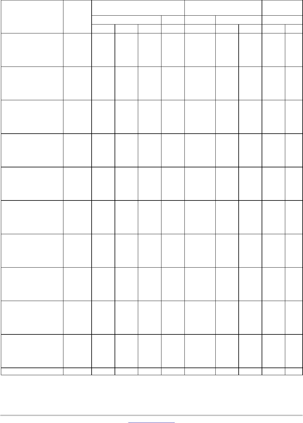
5% TOLERANCE FG ELECTRICAL CHARACTERISTICS (T
A
= 25°C unless otherwise noted, V
F
= 0.9 V Max. @ I
F
= 10 mA)
Device*
Device
Marking
Zener Voltage (Notes 3 and 4) Zener Impedance (Note 5)
Leakage Cur-
rent
V
Z
(Volts) @ I
ZT
Z
ZT
@ I
ZT
Z
ZK
@ I
ZK
I
R
@ V
R
Min Nom Max mA
W W
mA
mA
Volts
MMSZ5221BT1G C1 2.28 2.4 2.52 20 30 1200 0.25 100 1
MMSZ5222BT1G C2 2.38 2.5 2.63 20 30 1250 0.25 100 1
MMSZ5223BT1G C3 2.57 2.7 2.84 20 30 1300 0.25 75 1
MMSZ5224BT1G C4 2.66 2.8 2.94 20 30 1400 0.25 75 1
MMSZ5225BT1G C5 2.85 3.0 3.15 20 29 1600 0.25 50 1
MMSZ5226BT1G D1 3.14 3.3 3.47 20 28 1600 0.25 25 1
MMSZ5227BT1G D2 3.42 3.6 3.78 20 24 1700 0.25 15 1
MMSZ5228BT1G D3 3.71 3.9 4.10 20 23 1900 0.25 10 1
MMSZ5229BT1G D4 4.09 4.3 4.52 20 22 2000 0.25 5 1
MMSZ5230BT1G D5 4.47 4.7 4.94 20 19 1900 0.25 5 2
MMSZ5231BT1G E1 4.85 5.1 5.36 20 17 1600 0.25 5 2
MMSZ5232BT1G E2 5.32 5.6 5.88 20 11 1600 0.25 5 3
MMSZ5233BT1G E3 5.70 6.0 6.30 20 7 1600 0.25 5 3.5
MMSZ5234BT1G E4 5.89 6.2 6.51 20 7 1000 0.25 5 4
MMSZ5235BT1G E5 6.46 6.8 7.14 20 5 750 0.25 3 5
MMSZ5236BT1G F1 7.13 7.5 7.88 20 6 500 0.25 3 6
MMSZ5237BT1G F2 7.79 8.2 8.61 20 8 500 0.25 3 6.5
MMSZ5238BT1G F3 8.27 8.7 9.14 20 8 600 0.25 3 6.5
MMSZ5239BT1G F4 8.65 9.1 9.56 20 10 600 0.25 3 7
MMSZ5240BT1G F5 9.50 10 10.50 20 17 600 0.25 3 8
MMSZ5241BT1G H1 10.45 11 11.55 20 22 600 0.25 2 8.4
MMSZ5242BT1G/T3G H2 11.40 12 12.60 20 30 600 0.25 1 9.1
MMSZ5243BT1G H3 12.35 13 13.65 9.5 13 600 0.25 0.5 9.9
MMSZ5244BT1G H4 13.30 14 14.70 9.0 15 600 0.25 0.1 10
MMSZ5245BT1G H5 14.25 15 15.75 8.5 16 600 0.25 0.1 11
MMSZ5246BT1G J1 15.20 16 16.80 7.8 17 600 0.25 0.1 12
MMSZ5247BT1G J2 16.15 17 17.85 7.4 19 600 0.25 0.1 13
MMSZ5248BT1G J3 17.10 18 18.90 7.0 21 600 0.25 0.1 14
MMSZ5249BT1G J4 18.05 19 19.95 6.6 23 600 0.25 0.1 14
MMSZ5250BT1G J5 19.00 20 21.00 6.2 25 600 0.25 0.1 15
MMSZ5251BT1G K1 20.90 22 23.10 5.6 29 600 0.25 0.1 17
MMSZ5252BT1G K2 22.80 24 25.20 5.2 33 600 0.25 0.1 18
MMSZ5253BT1G K3 23.75 25 26.25 5.0 35 600 0.25 0.1 19
MMSZ5254BT1G K4 25.65 27 28.35 4.6 41 600 0.25 0.1 21
MMSZ5255BT1G K5 26.60 28 29.40 4.5 44 600 0.25 0.1 21
MMSZ5256BT1G M1 28.50 30 31.50 4.2 49 600 0.25 0.1 23
MMSZ5257BT1G M2 31.35 33 34.65 3.8 58 700 0.25 0.1 25
MMSZ5258BT1G/T3G M3 34.20 36 37.80 3.4 70 700 0.25 0.1 27
MMSZ5259BT1G M4 37.05 39 40.95 3.2 80 800 0.25 0.1 30
MMSZ5260BT1G M5 40.85 43 45.15 3.0 93 900 0.25 0.1 33
MMSZ5261BT1G N1 44.65 47 49.35 2.7 105 1000 0.25 0.1 36
MMSZ5262BT1G N2 48.45 51 53.55 2.5 125 1100 0.25 0.1 39
MMSZ5263BT1G N3 53.20 56 58.80 2.2 150 1300 0.25 0.1 43
MMSZ5264BT1G N4 57.00 60 63.00 2.1 170 1400 0.25 0.1 46
MMSZ5265BT1G N5 58.90 62 65.10 2.0 185 1400 0.25 0.1 47
MMSZ5266BT1G P1 64.60 68 71.40 1.8 230 1600 0.25 0.1 52
MMSZ5267BT1G P2 71.25 75 78.75 1.7 270 1700 0.25 0.1 56
MMSZ5268BT1G P3 77.90 82 86.10 1.5 330 2000 0.25 0.1 62
MMSZ5269BT1G P4 82.65 87 91.35 1.4 370 2200 0.25 0.1 68
MMSZ5270BT1G P5 86.45 91 95.55 1.4 400 2300 0.25 0.1 69
MMSZ5272BT1G/T3G R2 104.5 110 115.5 1.1 750 3000 0.25 0.1 84
3. “B” Suffix Type numbers shown have a standard tolerance of ±5% on the nominal Zener voltages.
4. Nominal Zener voltage is measured with the device junction in thermal equilibrium at T
L
= 30°C ±1°C.
5. Z
ZT
and Z
ZK
are measured by dividing the AC voltage drop across the device by the ac current applied.
The specified limits are for I
Z(AC)
= 0.1 I
Z(dc)
with the AC frequency = 1 kHz.
*Includes SZ-prefix devices where applicable.

MMSZ5231BT1G

Mfr. #:
Manufacturer:
ON Semiconductor
Description:
Zener Diodes 5.1V 500mW
Lifecycle:
New from this manufacturer.
Delivery:
DHL FedEx Ups TNT EMS
Payment:
T/T Paypal Visa MoneyGram Western Union