PIN # PIN NAME PIN TYPE DESCRIPTION
1 VDDA PWR 3.3V Power for the Analog Core
2 GNDA GND Ground for the Analog Core
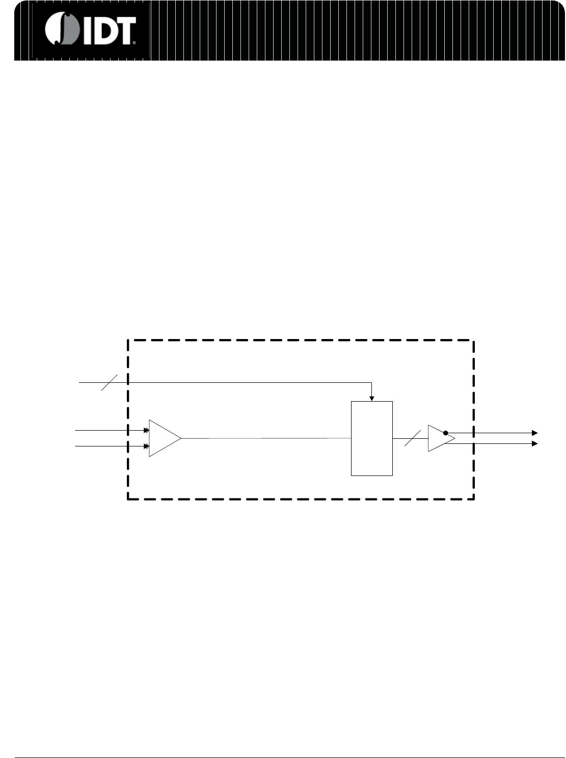
3OE3# IN
Output Enable for DIF3 output. Control is as follows:
0 = enabled, 1 = Low-Low
4 DIF3C_LPR OUT Complement clock of low power differential clock pair. (no 50ohm shunt resistor to GND needed)
5 DIF3T_LPR OUT True clock of low power differential clock pair. (no 50ohm shunt resistor to GND needed)
6 VDD_IO PWR Power supply for low power differential outputs, nominal 1.05V to 3.3V
7 GND GND Ground pin
8 DIF2C_LPR OUT Complement clock of low power differential clock pair. (no 50ohm shunt resistor to GND needed)
9 DIF2T_LPR OUT True clock of low power differential clock pair. (no 50ohm shunt resistor to GND needed)
10 OE2# IN
Output Enable for DIF2 output. Control is as follows:
0 = enabled, 1 = Low-Low
11 DIF1C_LPR OUT Complement clock of low power differential clock pair. (no 50ohm shunt resistor to GND needed)
12 DIF1T_LPR OUT True clock of low power differential clock pair. (no 50ohm shunt resistor to GND needed)
13 OE1# IN
Output Enable for DIF1 output. Control is as follows:
0 = enabled, 1 = Low-Low
14 GND GND Ground pin
15 VDD_IO PWR Power supply for low power differential outputs, nominal 1.05V to 3.3V
16 DIF0C_LPR OUT Complement clock of low power differential clock pair. (no 50ohm shunt resistor to GND needed)
17 DIF0T_LPR OUT True clock of low power differential clock pair. (no 50ohm shunt resistor to GND needed)
18 OE0# IN
Output Enable for DIF0 output. Control is as follows:
0 = enabled, 1 = Low-Low
19 DIF_INC IN Complement side of differential input clock
20 DIF_INT IN True side of differential input clock