6V31021NLGI

IDT6V31021
4-OUTPUT LOW POWER FANOUT BUFFER FOR PCIE GEN3 AND 10G ETHERNET
IDT®
4-OUTPUT LOW POWER FANOUT BUFFER FOR PCIE GEN3 AND 10G ETHERNET 4
IDT6V31021 REV A 121311
Absolute Maximum Ratings
Stresses above the ratings listed below can cause permanent damage to the IDT6V31021. These ratings, which are
standard values for IDT commercially rated parts, are stress ratings only. Functional operation of the device at these or any
other conditions above those indicated in the operational sections of the specifications is not implied. Exposure to absolute
maximum rating conditions for extended periods can affect product reliability. Electrical parameters are guaranteed only over
the recommended operating temperature range.
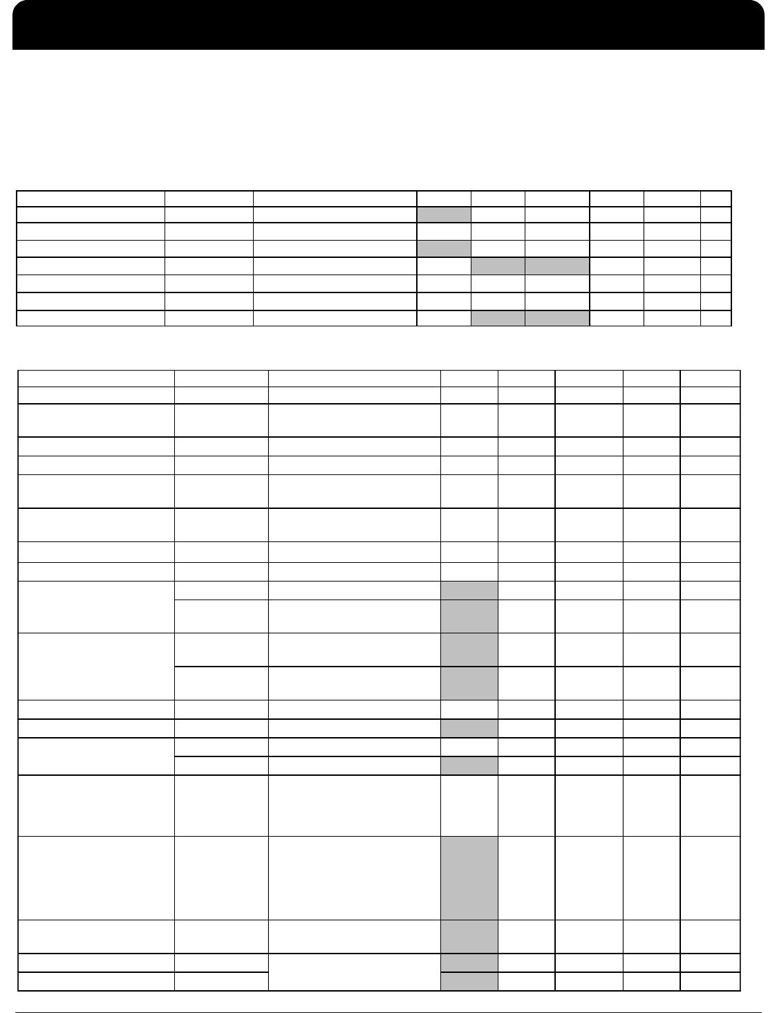
Electrical Characteristics–Input/Supply/Common Output Parameters
PARAMETER SYMBOL CONDITIONS MIN TYP MAX UNITS Notes
Maximum Supply Volta
e VDDA Core Supply Volta
g
e 4.6 V 1,7
Maximum Supply Voltage VDD_IO
Low-Voltage Differential I/O
0.99 3.8 V 1,7
Maximum Input Voltage
V
IH
3.3V LVCMOS Inputs 4.6 V 1,7,8
Minimum Input Voltage V
IL
Any Input Vss - 0.5 V 1,7
Ambient Operating Temp T
ambIN
D
Industrial Range -40 85 °C 1
Storage Temperature Ts - -65 150
°
C
1,7
Input ESD protection ESD prot Human Body Model 2000 V 1,7
PARAMETER SYMBOL CONDITIONS MIN TYP MAX UNITS Notes
Supply Voltage VDDA Supply Voltage 3.000 3.3 3.600 V 1
Supply Voltage VDDxxx_IO
Low-Voltage Differential I/O
Supply
0.99 1.05-3.3 3.600 V 1
Input High Voltage V
IHSE
Single-ended inputs 2 V
DD
+ 0.3 V 1
Input Low Voltage V
ILSE
Single-ended inputs V
SS
- 0.3 0.8 V 1
Differential Input High
Voltage
V
IHDI F
Differential inputs
(single-ended measurement)
600 1.15 V 1
Differential Input Low
Voltage
V
ILDIF
Differential inputs
(single-ended measurement)
V
SS
- 0.3 300 V 1
Input Slew Rate - DIF_IN dv/dt Measured differentially 0.4 8 V/ns 2
Input Leakage Current I
IN
V
IN
= V
DD ,
V
IN
= GND -5 5 uA 1
I
DD_3.3V
VDDA supply current 15 20 mA 1
I
DD_IO_133M
VDD_IO supply @ fOP =
133MHz
12 20 mA 1
I
DD_SB_3.3V
VDDA supply current, Input
stopped, OE# pins all high
500 750 uA 1
I
DD_SBIO
VDD_IO supply, Input
stopped, OE# pins all high
100 150 uA 1
Input Frequency F
i
V
DD
= 3.3 V 15 167 MHz 2
Pin Inductance L
p
in
7nH1
C
IN
Logic Inputs 1.5 5 pF 1
C
OUT
Output pin capacitance 6 pF 1
OE# latency
(at least one OE# is low)
T
OE#LAT
Number of clocks to enable
or disable output from
assertion/deassertion of OE#
1 2 3 periods 1
Clock stabilization time
(from all OE# high to first
OE# low).
T
STAB
Delay from assertion of first
OE# to first clock out
(assumes input clock running
and device in power down
state))
150 ns 1
Tdrive_OE# T
DROE#
Output enable after
OE# de-assertion
10 ns 1
Tfall_OE# T
FALL
5ns1
Trise_OE# T
RISE
5ns1
Power Down Current
(All OE# pins High)
Fall/rise time of OE# inputs
Input Capacitance
Operating Supply Current
IDT6V31021
4-OUTPUT LOW POWER FANOUT BUFFER FOR PCIE GEN3 AND 10G ETHERNET
IDT®
4-OUTPUT LOW POWER FANOUT BUFFER FOR PCIE GEN3 AND 10G ETHERNET 5
IDT6V31021 REV A 121311
AC Electrical Characteristics–DIF Low Power Differential Outputs
PARAMETER SYMBOL CONDITIONS MIN TYP MAX UNITS NOTES
Rising/Falling Edge Slew
Rate
t
SLR
Differential Measurement 1.5 2.2 4 V/ns 1,2
Slew Rate Variation t
SLVAR
Single-ended Measurement 13 20 % 1
Maximum Output Voltage V
HIGH
Includes overshoot 783 1150 mV 1
Minimum Output Voltage V
LOW
Includes undershoot -300 -22 mV 1
Differential Voltage Swing V
SWING
Differential Measurement 1200 mV 1
Crossing Point Voltage V
XABS
Single-ended Measurement 250 336 550 mV 1,3,4
Crossing Point Variation V
XABSVA
R
Single-ended Measurement 14 140 mV 1,3,5
Duty Cycle Distortion D
CYCDI S0
Differential Measurement,
fIN<=133.33MHz
1.6 3 % 1,6
Additive Cycle-to-Cycle
Jitter
DIFJ
C2CADD
Differential Measurement,
Additive
2.1 7 ps 1
DIF[3:0] Skew DIF
SKE
W
Differential Measurement 19 50 ps 1, 11
Propagation Delay t
PD
Input to output Delay 2.5 3.3 3.8 ns 1
Additive Phase Jitter -
PCIe Gen1
t
phase_addPCIG1
1.5MHz < 22MHz 1.6 6
ps
Pk-Pk
1,9
Additive Phase Jitter -
PCIe Gen2 High Band
t
phase_addPCIG2HI
High Band is 1.5MHz to
Nyquist (50MHz)
0.1 0.3 ps rms 1,9
Additive Phase Jitter -
PCIe Gen2 Low Band
t
phase_addPCIG2LO
Low Band is 10KHz to
1.5MHz
0.5 0.8 ps rms 1,9
Additive Phase Jitter -
PCIe Gen3
t
phase_addPCIG3
2MHz - 4MHz,
2MHz - 5MHz
0.19 0.3 ps rms 1,9
Additive Phase Jitter
161.1328125MHz =
10.3125G/64
t
phase_add10G/64
12KHz to 100MHz 60 100 fs rms 1,10
Notes on Electrical Characteristics (all measurements use R
S
=33ohms/C
L
=2pF test load):
1
Guaranteed by design and characterization, not 100% tested in production.
2
Slew rate measured through Vswing centered around differential zero
3
Vxabs is defined as the voltage where CLK = CLK#
4
Only applies to the differential rising edge (CLK rising and CLK# falling)
11
Mean value not including cycle-to-cycle jitter
10
Calculated from Agilent E5052A phase noise machine.
9
The 6V31021has no PLL, so the part itself contributes very little jitter to the input clock. But this also means that the 9DBL411 cannot 'de-jitter' a noisy
input clock. Values calculated per PCI SIG and per Intel Clock Jitter tool version 1.6.6. For PCIe RMS figures, additive jitter is calculated by solving the
following equation: Additive jitter = SQRT[(total jittter)^2 - (input jitter)^2]
8
Maximum input voltage is not to exceed maximum VDD
6
This figure refers to the maximum distortion of the input wave form.
5
Defined as the total variation of all crossing voltages of CLK rising and CLK# falling. Matching applies to rising edge rate of CLK and falling edge of
CLK#. It is measured using a +/-75mV window centered on the average cross point where CLK meets CLK#.
7
Operation under these conditions is neither implied, nor guaranteed.
IDT6V31021
4-OUTPUT LOW POWER FANOUT BUFFER FOR PCIE GEN3 AND 10G ETHERNET
IDT®
4-OUTPUT LOW POWER FANOUT BUFFER FOR PCIE GEN3 AND 10G ETHERNET 6
IDT6V31021 REV A 121311
Marking Diagram
Notes:
1. ‘**’ is the lot sequence.
2. ‘$’ is the mark code.
3. ‘YWW’ is the year and week that the part was assembled.
4. ‘G’ denotes RoHS compliant package.
5. ‘I’ denotes industrial temperature range.
6. Bottom marking: country of origin if not USA.
6V310
21NLGI
YWW**$

6V31021NLGI

Mfr. #:
Manufacturer:
IDT
Description:
Clock Buffer PCIE BUFFER - GEN2 - LOW POWER
Lifecycle:
New from this manufacturer.
Delivery:
DHL FedEx Ups TNT EMS
Payment:
T/T Paypal Visa MoneyGram Western Union

Products related to this Datasheet