PDF: 09005aef837131bb/Source: 09005aef8086ea0b Micron Technology, Inc., reserves the right to change products or specifications without notice.
dd4c16_32x64h.fm - Rev. E 10/08 EN
10 ©2003 Micron Technology, Inc. All rights reserved.
128MB, 256MB (x64, SR) 200-Pin DDR SDRAM SODIMM
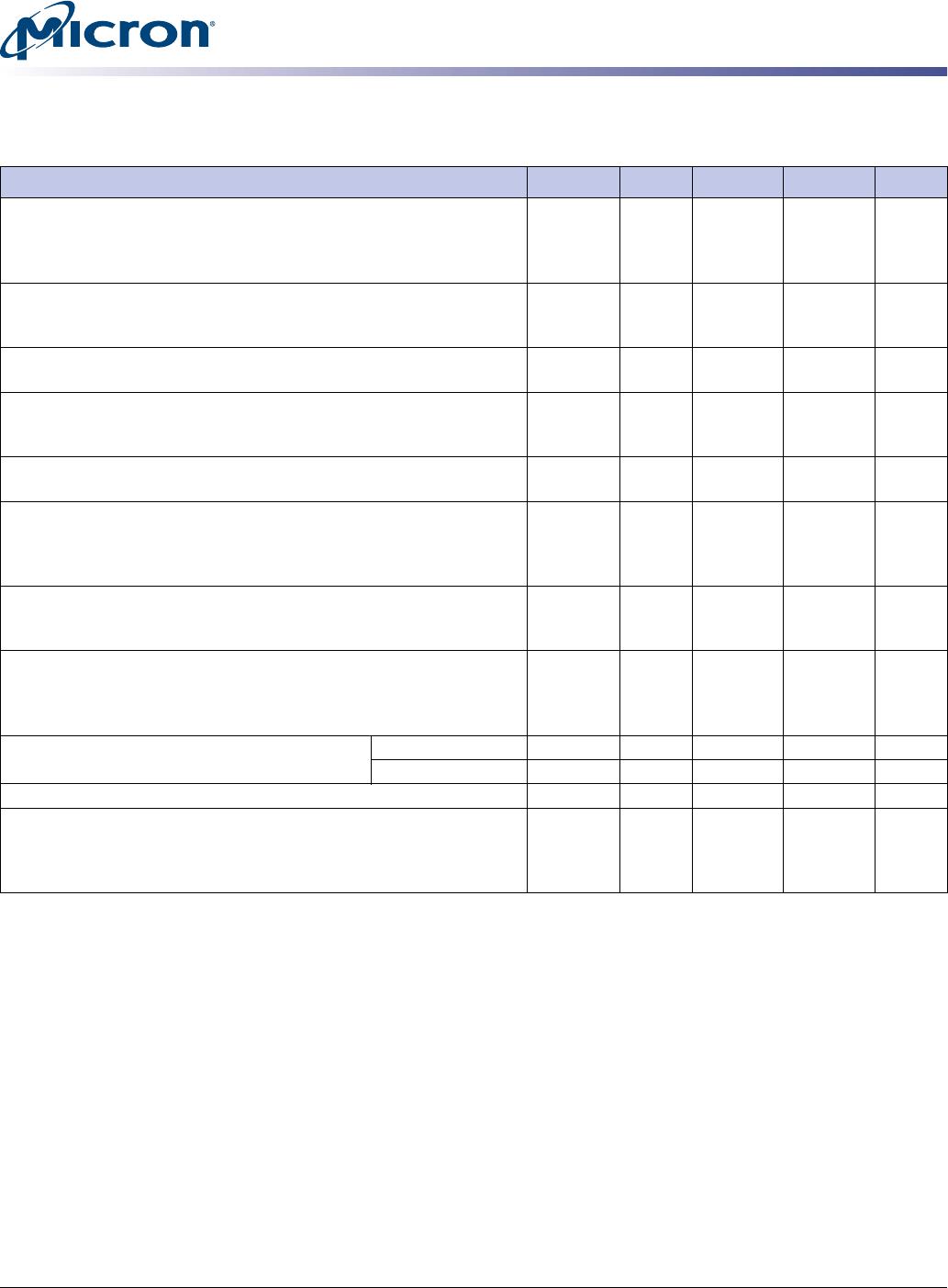
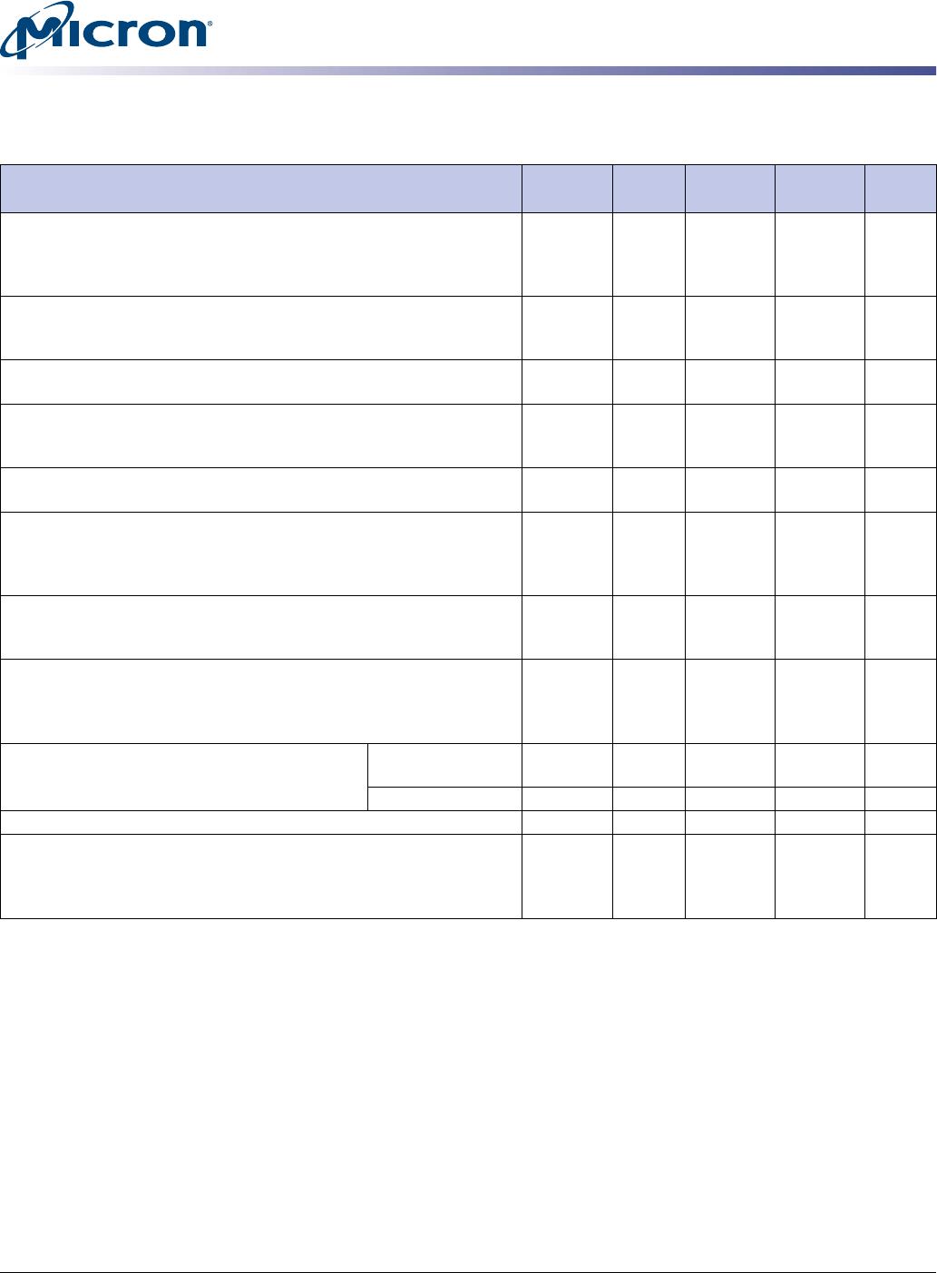
Idd Specifications
Table 10: Idd Specifications and Conditions – 128MB (All Other Die Revisions)
Values are for the MT46V16M16 DDR SDRAM only and are computed from values specified in the
256Mb (16 Meg x 16) component data sheet
Parameter/Condition Symbol -40B -335
-26A/
-265
Units
Operating one bank active-precharge current:
t
RC =
t
RC (MIN);
t
CK =
t
CK (MIN); DQ, DM, and DQS inputs changing
once per clock cycle; Address and control inputs changing once
every two clock cycles
Idd0 540 500 480 mA
Operating one bank active-read-precharge current:
BL = 4;
t
RC =
t
RC (MIN);
t
CK =
t
CK (MIN); Iout= 0mA; Address and
control inputs changing once per clock cycle
Idd1 740 720 620 mA
Precharge power-down standby current: All device banks idle;
Power-down mode;
t
CK =
t
CK (MIN); CKE = (LOW)
Idd2P 16 16 16 mA
Idle standby current: CS# = HIGH; All device banks idle;
t
CK=
t
CK(MIN); C KE = HIGH; Address and other control inputs
changing once per clock cycle; Vin = Vref for
DQ, DM, and DQS
Idd2F 240 200 180 mA
Active power-down standby current: One device bank active;
Power-down mode;
t
CK =
t
CK (MIN); CKE = LOW
Idd3P 160 120 100/
120
mA
Active standby current: CS# = HIGH; CKE = HIGH; One device
bank;
t
RC =
t
RAS (MAX);
t
CK =
t
CK (MIN); DQ, DM, and DQS inputs
changing twice per clock cycle; Address and other control inputs
changing once per clock cycle
Idd3N 280 240 200 mA
Operating burst read current: BL = 2; Continuous burst reads;
One device bank active; Address and control inputs changing once
per clock cycle;
t
CK =
t
CK (MIN); Iout = 0mA
Idd4R 1040 880 740 mA
Operating burst write current: BL = 2; Continuous burst writes;
One device bank active; Address and control inputs changing once
per clock cycle;
t
CK =
t
CK (MIN); DQ, DM, and DQS inputs changing
twice per clock cycle
Idd4W 860 780 640 mA
Auto refresh current
t
RFC =
t
RFC (MIN)
Idd5 1040 1020 940/
980
mA
t
RFC = 7.8125µs
Idd5A 24 24 24 mA
Self refresh current: CKE ≤ 0.2V
Idd6 16 16 16 mA
Operating bank interleave read current: Four device bank
interleaving (BL = 4) with auto precharge;
t
RC =
t
RC (MIN);
t
CK =
t
CK
(MIN); Address and control inputs change only during active READ
or WRITE commands
Idd7 2046 1760 1520/
1600
mA