12
Testing Digital Fiber Optic Links
The overall performance of a complete digital fiber optic
link can be determined by stimulating the transmitter
with a pseudo random bit sequence (PRBS) data source
while observing the response at the receiver’s output. A
PRBS data source is a shift register where data bits from
two or more shift register stages are combined using an
exclusive-or gate. When a clock signal is applied to the CLK
input of the shift register, and the output of the exclusive
OR gate is applied to the D
S
input of the shift register, the
PRBS generator produces a serial bit stream which appears
to be random, but is actually periodic and reproducible. If
the PRBS generator is constructed using a 23 bit long shift
register, the exclusive OR feedback can be configured so
that the shift register will be in one of 2
23
-1 possible states
at any given clock time. The 2
23
-1 PRBS data generator
appears to be a source of random serial data, but it is
actually the output of a shift register which is in one of
8,388,610 precisely repeatable states. PRBS generators
send an exactly repeating serial data pattern that can be
checked bit-by-bit to determine if the fiber optic link made
errors while transporting the data. A bit-error-ratio test set
is an instrument which contains a PRBS generator, a bit-by-
bit error detector, and an error counter. Bit-error-ratio test
sets measure the probability that the fiber optic link will
make an error. Probability of error is commonly expressed
as a bit-error-ratio or BER. The BER is simply the number of
errors which occurred divided by the number of bits trans-
mitted through the fiber optic link in some arbitrary time
interval.
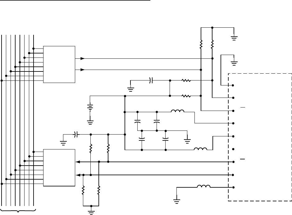
The +5 V ECL interface of the transceiver shown in Figure
8 is convenient for use with off-the-shelf VLSI chips like the
TAXIchip, but it is not compatible with the majority of the
test equipment used to measure the performance of fiber
optic links. Most bit error rate (BER) test sets have conven-
tional -5 V ECL inputs and outputs. The test fixture shown in
Figure 12 provides a convenient way to convert +5 V ECL to
-5 V ECL. This test fixture allows the transceiver in Figure 8
to be used with any BER test set (BER machine) with a con-
ventional -5V ECL interface. The test fixture in Figure 12
was used to collect the performance data shown in this
application note.
The waveforms shown in Figures 13 and 14 are known as
eye diagrams. These eye diagrams were measured by con-
necting a digitizing oscilloscope, with a 1 GHz bandwidth,
to the receiver’s +5 V ECL output. The Agilent 54100A
oscilloscope used for these measurements was triggered
from the PRBS generator’s clock. The lack of correla-
tion between the oscilloscope’s time base, and the PRBS
generator’s clock, assures that the oscilloscope will ran-
domly sample the PRBS data. The infinite persistence mode
of the Agilent 54100A Digitizing Oscilloscope was used,
and the electrical output of the receiver was measured
for roughly 1 hour, to determine the eye opening. As eye
opening, or eye width, increases, the probability that the
fiber optic link will make an error decreases. A wide eye
opening makes it easier to extract the clock signal which is
normally encoded with the data passing through the serial
communication channel. Fiber optic links are less likely to
make errors when the eye is wide open, because there is
more time for the clock to synchronously detect the data
while it is stable and unchanging.
The results shown in Figure 13 were obtained at room
temperature when 125 MBd PRBS data was transmitted
through a plastic fiber optic link. Figure 13 shows that the
eye opening is typically 5.52 ns when the recommended
transceiver in Figure 8 is used with 20 m of 1 mm plastic
fiber. Excellent performance can also be achieved by using
the transceiver in Figure 8 with Avago’s 200 µm HCS
TM
fiber.
Figure 14 indicates that the eye opening is typically 5.56 ns
wide when 125 MBd data is transmitted through 100 m of
200 µm HCS
TM
fiber.
A better method for measuring the performance of a
complete optical data link is to use a computer controlled
delay line and a BER test set. This technique uses a com-
puter to adjust the delay of the BER test set’s clock relative
to the PRBS data. At a data rate of 125 MBd the clock delay
was changed in 100 ps increments. The test system then
measures and stores the probability of error at each 100
ps delay step until the clock has been swept through the
entire 8.0 ns period of every 125 MBd symbol transmitted
through the fiber optic link. The results in Figure 15 were
obtained when the BER test set applied 2
23
-1 PRBS data
to the transmitter portion of the transceiver under evalu-
ation. Figure 15 shows that when using the transceiver
recommended in Figure 8 BER is typically ≤ 1 x 10
-10
for 5.8
ns of each pseudo random symbol transmitted through
a 20 m length of 1 mm plastic fiber. The optical power
applied to the receiver was Pr = -16.4 dBm average for the
measured results shown in Figure 15. Figure 16 shows the
performance that can be achieved at 125 MBd with 200
µm HCS
TM
fiber. Figure 16 shows that when using the trans-
ceiver recommended in Figure 8, BER will be typically ≤ 1 x
10
-10
for 5.3 ns of each pseudo random symbol transmitted
through a 100 m length of 200 µm HCS
TM
fiber. The optical
power applied to the receiver was Pr = -18.0 dBm average
for the measured results shown in Figure 16.