20
For more information www.linear.com/LTC2631
operation
The LTC2631 is a family of single voltage-output DACs
in 8-lead ThinSOT packages. Each DAC can operate rail-
to-rail using an external reference, or with its full-scale
voltage set by an integrated reference. Twelve combina
-
tions of accuracy (12-, 10-, and 8-bit), power-on reset
value (
zero or mid-scale), and full-scale voltage (2.5V or
4.096V) are available. The LTC2631 is controlled using a
2-wire I
2
C interface.
Power-On Reset
The LTC2631-HZ/LTC2631-LZ clear the output to zero-
scale when power is first applied, making system initial
-
ization consistent and repeatable.
For some
applications, downstream circuits are active
during DAC power-up, and may be sensitive to nonzero
outputs from the DAC during this time. The LTC2631
contains circuitry to reduce the power-on glitch: the ana
-
log output
typically rises less than 5mV above zero-scale
during power
on if the power supply is ramped to 5V in
1ms or more. In general, the glitch amplitude decreases as
the power supply ramp time is increased. See “Power-On
Reset Glitch” in the Typical Performance Characteristics
section.
The LTC2631-HM/LTC2631-LM provide an alternative
reset, setting the output
to mid-scale when power is first
applied.
Default reference
mode selection is described in the Ref-
erence Modes section.
Power Supply Sequencing
The voltage at REF (Pin 6) should be kept within the range
– 0.3V ≤ V
REF
≤ V
CC
+ 0.3V (see Absolute Maximum Rat-
ings). Particular care
should be taken to observe these
limits during power supply turn-on and turn-off sequences,
when the voltage at V
CC
(Pin 5) is in transition.
Transfer Function
The digital-to-analog transfer function is
V
OUT(IDEAL)
=
2
N
V
REF
where k is the decimal equivalent of the binary DAC input
code, N is the resolution, and V
REF
is either 2.5V (LTC2631-
LM/LTC2631-LZ) or 4.096V (LTC2631-HM/LTC2631-HZ)
when in Internal Reference mode, and the voltage at REF
(Pin 6) when in External Reference mode.
I
2
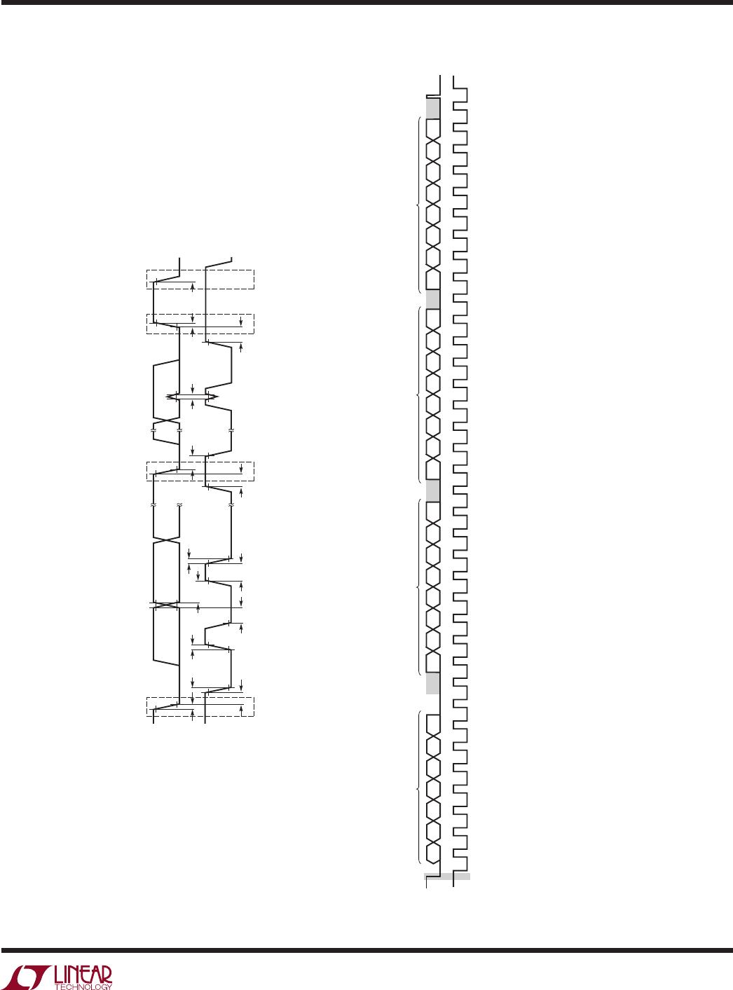
C Serial Interface
The LTC2631 communicates with a host using the stan-
dard 2-wire I
2
C interface. The Timing Diagrams (Figures 1
and 2) show the timing
relationship of the signals on the
bus. The two bus lines, SDA and SCL, must be high when
the bus is not in use. External pull-up resistors or current
sources are required on these lines. The value of these
pull-up resistors is dependent on the power supply and
can be obtained from the I
2
C specifications. For an I
2
C
bus operating in the fast mode, an active pull-up will be
necessary if the bus capacitance is greater than 200pF.
The LTC2631 is a receive-only (slave) device. The master
can write to the LTC2631. The LTC2631 does not respond
to a read from the master.
START (S) and STOP (P) Conditions
When the bus is not
in use, both SCL and SDA must be
high. A bus master signals the beginning of a communi-
cation to
a slave device by transmitting a START condition.
A START condition is generated by transitioning SDA from
high to low while SCL is high.
When the master has finished communicating with the
slave, it issues a STOP condition. A STOP condition is
generated by transitioning SDA from low to high while
SCL is high. The bus is then free for communication with
another I
2
C device.
Acknowledge
The Acknowledge signal is used for handshaking between
the master and the slave. An Acknowledge (active LOW)
generated by the slave lets the master know that the latest
byte of information was properly received. The Acknowl
-
edge related clock pulse is generated by the master. The
master releases the SDA line (HIGH) during the Acknowl-
edge clock
pulse. The slave-receiver must pull down the
SDA bus
line during the Acknowledge clock pulse so that
it remains a stable LOW during the HIGH period of this
clock pulse. The LTC2631 responds to a write by a master