5
For more information www.linear.com/LTC2631
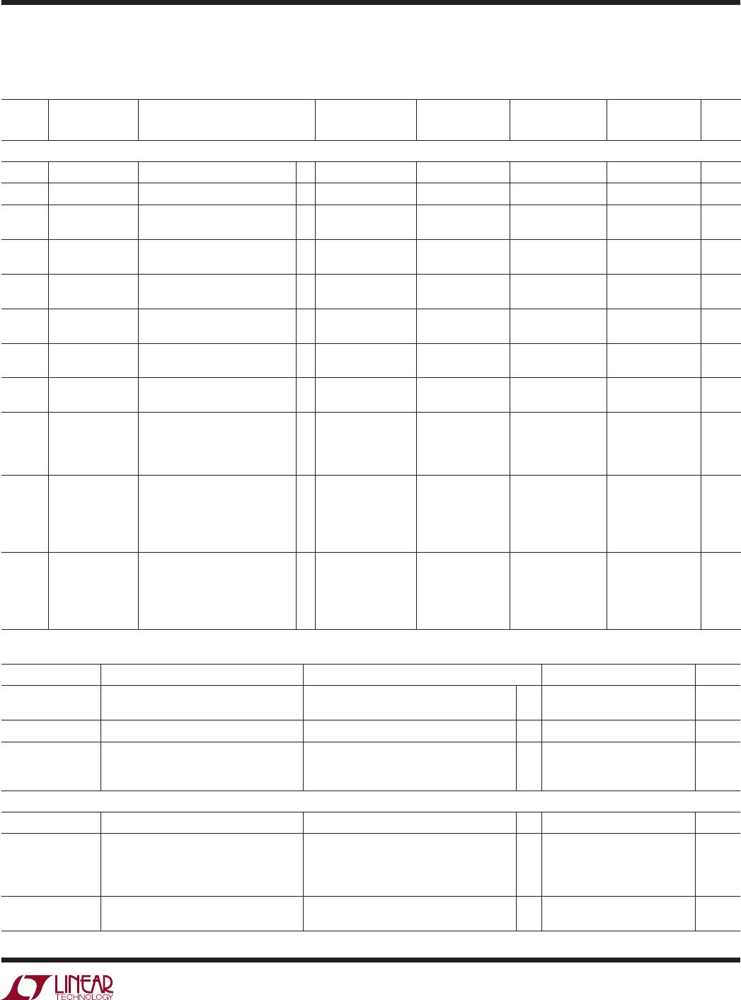
electrical characteristics
LTC2631-8 LTC2631-10 LTC2631-12 LTC2631A-12
SYMBOL PARAMETER CONDITIONS MIN TYP MAX MIN TYP MAX MIN TYP MAX MIN TYP MAX UNITS
DC Performance
Resolution
l
8 10 12 12 Bits
Monotonicity V
CC
= 3V, Internal Ref. (Note 4)
l
8 10 12 12 Bits
DNL Differential
Nonlinearity
V
CC
= 3V, Internal Ref. (Note 4)
l
±0.5 ±0.5 ±1 ±1 LSB
INL Integral
Nonlinearity
V
CC
= 3V, Internal Ref. (Note 4)
l
±0.05 ±0.5 ±0.2 ±1 ±1 ±2.5 ±0.5 ±1 LSB
ZSE Zero-Scale Error V
CC
= 3V, Internal Ref.,
Code = 0
l
0.5 5 0.5 5 0.5 5 0.5 5 mV
V
OS
Offset Error V
CC
= 3V, Internal Ref.
(Note 5)
l
±0.5 ±5 ±0.5 ±5 ±0.5 ±5 ±0.5 ±5 mV
V
OSTC
V
OS
Temperature
Coefficient
V
CC
= 3V, Internal Ref.
(Note 5)
±10 ±10 ±10 ±10 µV/°C
FSE Full-Scale Error
V
CC
= 3V, Internal Ref.
(Note 15)
l
±0.08 ±0.4 ±0.08 ±0.4 ±0.08 ±0.4 ±0.08 ±0.4 %FSR
V
FSTC
Full-Scale
Voltage
Temperature
Coefficient
V
CC
= 3V, Internal Ref. (Note 10)
C-Grade
I-Grade
H-Grade
±10
±10
±10
±10
±10
±10
±10
±10
±10
±10
±10
±10
ppm/°C
ppm/°C
ppm/°C
Load Regulation Internal Ref., Mid-Scale,
V
CC
= 3V ±10%,
–5mA ≤ I
OUT
≤ 5mA,
V
CC
= 5V ±10%,
–10mA ≤ I
OUT
≤ 10mA
l
l
0.009
0.009
0.016
0.016
0.035
0.035
0.064
0.064
0.14
0.14
0.256
0.256
0.14
0.14
0.256
0.256
LSB/mA
LSB
/mA
R
OUT
DC Output
Impedance
Internal Ref., Mid-Scale,
V
CC
= 3V ±10%,
–5mA ≤ I
OUT
≤ 5mA,
V
CC
= 5V ±10%,
–10mA ≤ I
OUT
≤ 10mA
l
l
0.09
0.09
0.156
0.156
0.09
0.09
0.156
0.156
0.09
0.09
0.156
0.156
0.09
0.09
0.156
0.156
Ω
Ω
The l denotes the specifications which apply over the full operating
temperature range, otherwise specifications are at T
A
= 25°C. V
CC
= 2.7V to 5.5V, V
OUT
unloaded unless otherwise specified.
LTC2631-LM12/-LM10/-LM8/-LZ12/-LZ10/-LZ8, LTC2631A-LM12/-LZ12 (V
FS
= 2.5V)
SYMBOL PARAMETER CONDITIONS MIN TYP MAX UNITS
V
OUT
DAC Output Span External Reference
Internal Reference
0 to V
REF
0 to 2.5
V
V
PSR Power Supply Rejection V
CC
= 3V ±10% or 5V ±10% –80 dB
I
SC
Short-Circuit Output Current (Note 6)
Sinking
Sourcing
V
FS
= V
CC
= 5.5V
Zero-Scale; V
OUT
shorted to V
CC
Full-Scale; V
OUT
shorted to GND
l
l
27
–28
48
–48
mA
mA
Power Supply
V
CC
Positive Supply Voltage For Specified Performance
l
2.7 5.5 V
I
CC
Supply Current (Note 7) V
CC
= 3V, V
REF
= 2.5V, External Reference
V
CC
= 3V, Internal Reference
V
CC
= 5V, V
REF
= 2.5V, External Reference
V
CC
= 5V, Internal Reference
l
l
l
l
150
180
160
190
200
240
210
260
µA
µA
µA
µA
I
SD
Supply Current in Power-Down Mode
(Note 7)
V
CC
= 5V, C-Grade, I-Grade
V
CC
= 5V, H-Grade
l
l
0.6
0.6
1.8
4
µA
µA

