Micrel, Inc. MIC5219
June 2009 10 M0371-061809
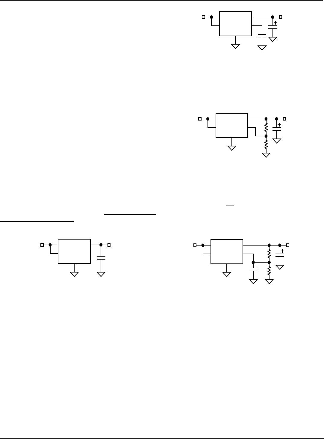
Peak Current Applications
The MIC5219 is designed for applications where high start-up
currents are demanded from space constrained regulators.
This device will deliver 500mA start-up current from a SOT-
23-5 or MM8 package, allowing high power from a very low
prole device. The MIC5219 can subsequently provide output
current that is only limited by the thermal characteristics of
the device. You can obtain higher continuous currents from
the device with the proper design. This is easily proved with
some thermal calculations.
If we look at a specic example, it may be easier to follow.
The MIC5219 can be used to provide up to 500mA continuous
output current. First, calculate the maximum power dissipa-
tion of the device, as was done in the thermal considerations
section. Worst case thermal resistance (θ
JA
= 220°C/W for
the MIC5219-x.xBM5), will be used for this example.
P
D
(max ) =
T
J
(max ) − T
A
( )
θ
JA
Assuming a 25°C room temperature, we have a maximum
power dissipation number of
P
D
(max ) =
125 °C − 25°C
( )
220 °C /W
P
D
(max) = 455mW
Then we can determine the maximum input voltage for a
5-volt regulator operating at 500mA, using worst case ground
current.
P
D
(max) = 455mW = (V
IN
– V
OUT
) I
OUT
+ V
IN
I
GND
I
OUT
= 500mA
V
OUT
= 5V
I
GND
= 20mA
455mW = (V
IN
– 5V) 500mA + V
IN
× 20mA
2.995W = 520mA × V
IN
V
IN
(max ) =
2.955W
520mA
= 5.683V
Therefore, to be able to obtain a constant 500mA output cur-
rent from the 5219-5.0BM5 at room temperature, you need
extremely tight input-output voltage differential, barely above
the maximum dropout voltage for that current rating.
You can run the part from larger supply voltages if the proper
precautions are taken. Varying the duty cycle using the en-
able pin can increase the power dissipation of the device by
maintaining a lower average power gure. This is ideal for
applications where high current is only needed in short bursts.
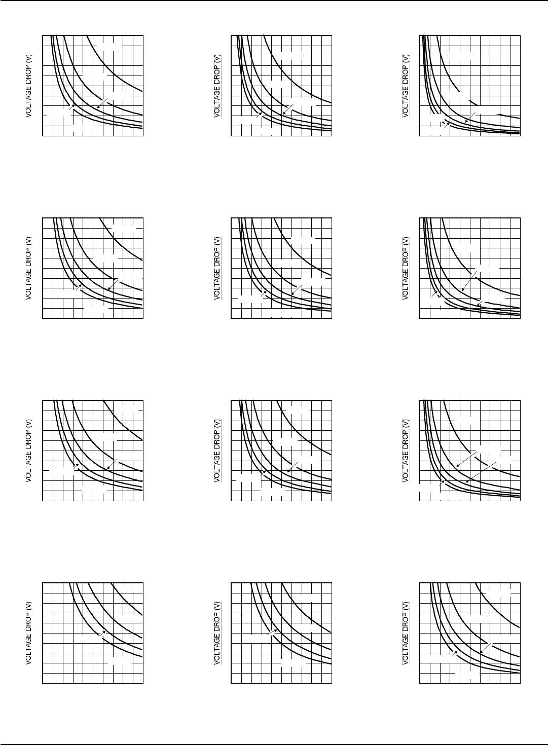
Figure 1 shows the safe operating regions for the MIC5219-x.
xBM5 at three different ambient temperatures and at differ-
ent output currents. The data used to determine this gure
assumed a minimum footprint PCB design for minimum heat
sinking. Figure 2 incorporates the same factors as the rst
gure, but assumes a much better heat sink. A 1" square cop-
per trace on the PC board reduces the thermal resistance of
the device. This improved thermal resistance improves power
dissipation and allows for a larger safe operating region.
Figures 3 and 4 show safe operating regions for the MIC5219-x.
xBMM, the power MSOP package part. These graphs show
three typical operating regions at different temperatures. The
lower the temperature, the larger the operating region. The
graphs were obtained in a similar way to the graphs for the
MIC5219-x.xBM5, taking all factors into consideration and
using two different board layouts, minimum footprint and 1"
square copper PC board heat sink. (For further discussion
of PC board heat sink characteristics, refer to “Application
Hint 17, Designing PC Board Heat Sinks” .)
The information used to determine the safe operating regions
can be obtained in a similar manner such as determining
typical power dissipation, already discussed. Determining
the maximum power dissipation based on the layout is the
rst step, this is done in the same manner as in the previous
two sections. Then, a larger power dissipation number multi-
plied by a set maximum duty cycle would give that maximum
power dissipation number for the layout. This is best shown
through an example. If the application calls for 5V at 500mA
for short pulses, but the only supply voltage available is
8V, then the duty cycle has to be adjusted to determine an
average power that does not exceed the maximum power
dissipation for the layout.
Avg.P
D
=
% DC
100
V
IN
– V
OUT
( )
I
OUT
+V
IN
I
GND
455mW =
% DC
100
8V – 5V
( )
500mA + 8V × 20mA
455mW =
% Duty Cycle
100
1.66W
With an output current of 500mA and a three-volt drop across
the MIC5219-xxBMM, the maximum duty cycle is 27.4%.
Applications also call for a set nominal current output with a
greater amount of current needed for short durations. This is a
tricky situation, but it is easily remedied. Calculate the average
power dissipation for each current section, then add the two
numbers giving the total power dissipation for the regulator.
For example, if the regulator is operating normally at 50mA,
but for 12.5% of the time it operates at 500mA output, the
total power dissipation of the part can be easily determined.
First, calculate the power dissipation of the device at 50mA.
We will use the MIC5219-3.3BM5 with 5V input voltage as
our example.
P
D
× 50mA = (5V – 3.3V) × 50mA + 5V × 650µA
P
D
× 50mA = 173mW
However, this is continuous power dissipation, the actual
on-time for the device at 50mA is (100%-12.5%) or 87.5%
of the time, or 87.5% duty cycle. Therefore, P
D
must be mul-
tiplied by the duty cycle to obtain the actual average power
dissipation at 50mA.