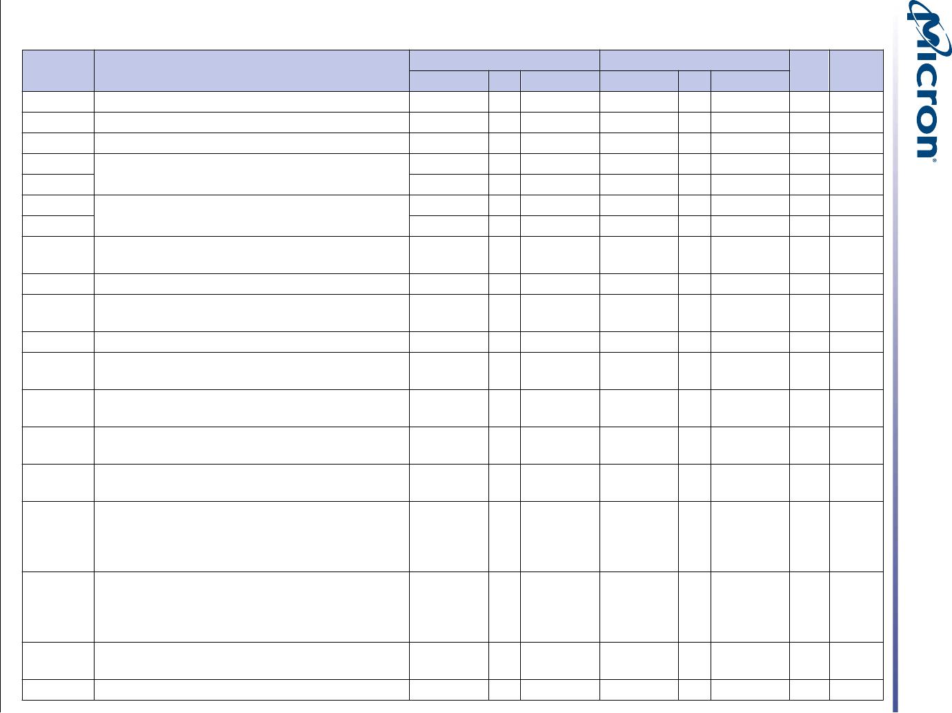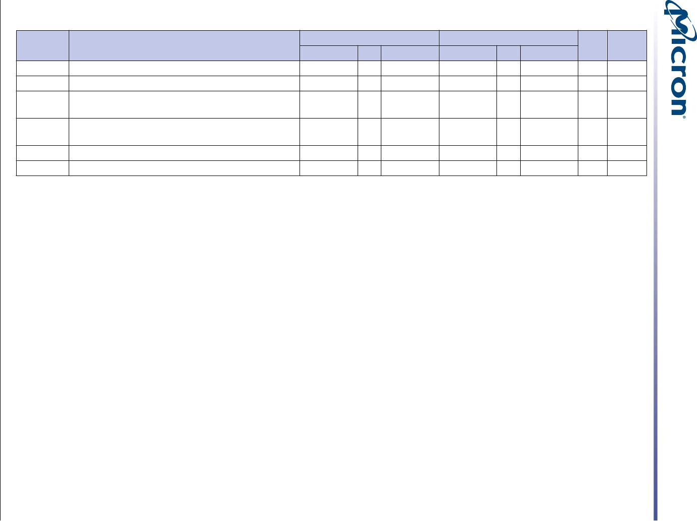
Table 6: DC Operating Conditions (Continued)
Symbol Parameter
POD135 POD125
Unit NotesMin Typ Max Min Typ Max
V
IDCK(DC)
CK_t, CK_c clock input differential voltage 0.198 – – 0.18 − − V 10, 12
V
IDWCK(DC)
WCK_t, WCK_c clock input differential voltage 0.18 – – 0.165 − − V 11, 13
I
L
Input leakage current (any input 0V ≤ V
IN
≤ V
DDQ
; all
other signals not under test = 0V)
–5 – 5 −5 − 5 µA
I
OZ
Output leakage current (outputs are disabled; 0V ≤
V
OUT
≤ V
DDQ
)
–5 – 5 −5 − 5 µA
V
OL(DC)
Output logic low voltage – – 0.56 – – 0.52 V
ZQ External resistor value 115 120 125 115 120 125 Ω
Notes:
1. GDDR6 SGRAM devices are designed to tolerate PCB designs with separate V
DD
and V
DDQ
power regulators.
2. DC bandwidth is limited to 20 MHz.
3. AC noise in the system is estimated at 50mV peak-to-peak for the purpose of DRAM design.
4. The reference voltage source and control for DQ and DBI_n pins are determined by half V
REFD
, and V
REFD
level
mode register bits.
5. Programmable V
REFD
levels are not supported with V
REFD2
.
6. The reference voltage source (external or internal) is determined at power‐up; the reference voltage level is deter-
mined by half V
REFC
and the V
REFC
offset mode register bit.
7. Programmable V
REFC
offsets are not supported with V
REFC2
.
8. V
IHR
and V
ILR
apply to boundary scan input pins TDI, TMS, and TCK. V
IHR
and V
ILR
apply to EDC and CA inputs at
reset when latching default device configurations. V
IHR
and V
ILR
also apply to CA, CABI_n, CKE_n, CK, DQ, DBI_n,
EDC, and WCK inputs when boundary scan mode is active and input data are latched in the capture-DR TAP con-
troller state.
9. This provides a minimum of 0.845V to a maximum of 1.045V with POD135, and a minimum of 0.775V to a maxi-
mum of 0.975V with POD125, and is normally 70% of V
DDQ
. DRAM timings relative to CK cannot be guaranteed if
these limits are exceeded.
10. V
IDCK
is the magnitude of the difference between the input level in CK_t and the input level on CK_c. The input
reference level for signals other than CK_t and CK_c is V
REFC
.
11. V
IDWCK
is the magnitude of the difference between the input level in WCK_t and the input level on WCK_c. The
input reference level for signals other than WCK_t and WCK_c is either V
REFC
, V
REFC2
, V
REFD
, or V
REFD2
.
12. The CK_t and CK_c input reference level (for timing referenced to CK_t and CK_c) is the point at which CK_t and
CK_c cross. Refer to the applicable timings in the AC Timings table.
13. The WCK_t and WCK_c input reference level (for timing referenced to WCK_t and WCK_c) is the point at which
WCK_t and WCK_c cross. Refer to the applicable timings in the AC Timings table.
14. Use V
IHR
and V
ILR
when boundary scan mode is active and input data are latched in the capture-DR TAP controller
state.
8Gb: 2 Channels x16/x8 GDDR6 SGRAM
Operating Conditions
CCMTD-1412786195-10191
gddr6_sgram_8gb_brief.pdf - Rev. F 8/18 EN
17
Micron Technology, Inc. reserves the right to change products or specifications without notice.
© 2016 Micron Technology, Inc. All rights reserved.