Table 1: 180-Ball FBGA Ball Descriptions
Symbol Type Description
CK_t,
CK_c
Input Clock: CK_t and CK_c are differential clock inputs. CK_t and CK_c do not have chan-
nel indicators as one clock is shared between both channel A and channel B on a de-
vice. Command address (CA) inputs are latched on the rising and falling edge of CK.
All latencies are referenced to CK.
WCK_t,
WCK_c
Input Write clock: WCK_t and WCK_c are differential clocks used for write data capture
and read data output. WCK_t/WCK_c are associated with DQ[15:0], DBI[1:0]_n, and
EDC[1:0].
CKE_n Input Clock enable: CKE_n LOW activates and CKE_n HIGH deactivates the internal clock,
device input buffers, and output drivers excluding RESET_n, TDI, TDO, TMS, and TCK.
Taking CKE_n HIGH provides PRECHARGE POWER-DOWN and SELF REFRESH opera-
tions (all banks idle), or ACTIVE POWER-DOWN (row ACTIVE in any bank). CKE_n
must be maintained LOW throughout read and write accesses.
CA[9:0] Input Command address (CA): The CA inputs receive packetized DDR command, address
or other information, for example, the op-code for the MRS command. See Com-
mand Truth Table for details.
CABI_n Input Command address bus inversion
DQ[15:0] I/O Data input/output: Bidirectional 16-bit data bus.
DBI[1:0]_n I/O Data bus inversion: DBI0_n is associated with DQ[7:0], DBI1_n is associated with
DQ[15:8].
EDC[1:0] Output Error detection code: The calculated CRC data is transmitted on these signals. In
addition these signals drive a "hold" pattern when idle. EDC0 is associated with
DQ[7:0], EDC1 is associated with DQ[15:8].
V
DDQ
Supply I/O power supply: Isolated on the die for improved noise immunity.
V
DD
Supply Power supply
V
SS
Supply Ground
V
PP
Supply Pump voltage
V
REFC
Supply Reference voltage for CA, CABI_n, and CKE_n signals
ZQ Reference External reference for auto calibration
TDI Input JTAG test data input
TDO Output JTAG test data output
TMS Input JTAG test mode select
TCK Input JTAG test clock
RESET_n Input Reset: RESET_n low asynchronously initiates a full chip reset. With RESET_n LOW all
ODTs are disabled. A full chip reset may be performed at any time by pulling RE-
SET_n LOW.
NC – No connect
Note:
1. Index "_A" or "_B" represents the channel indicator "A" and "B" of the device. Signal
names including the channel indicator are used whenever more than one channel is ref-
erenced, for example, with the ball assignment. The channel indicator is omitted when-
ever features and functions common to both channels are described.
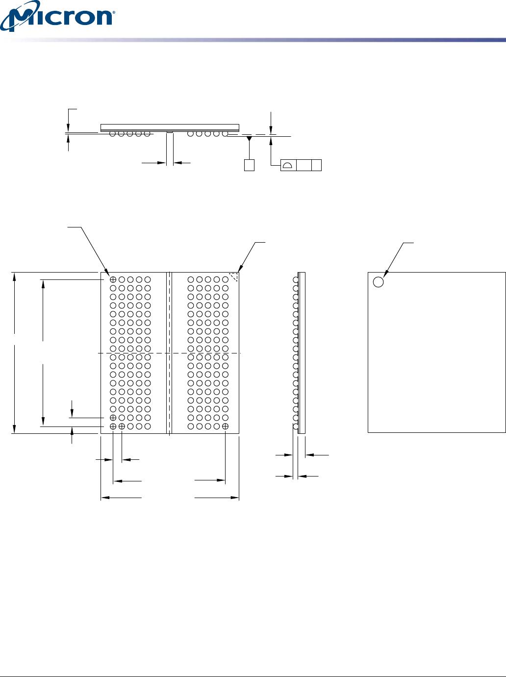
8Gb: 2 Channels x16/x8 GDDR6 SGRAM
Ball Assignments and Descriptions
CCMTD-1412786195-10191
gddr6_sgram_8gb_brief.pdf - Rev. F 8/18 EN
4
Micron Technology, Inc. reserves the right to change products or specifications without notice.
© 2016 Micron Technology, Inc. All rights reserved.