Design and specifications are each subject to change without notice. Ask factory for the current technical specifications before purchase and/or use.
Should a safety concern arise regarding this product, please be sure to contact us immediately.
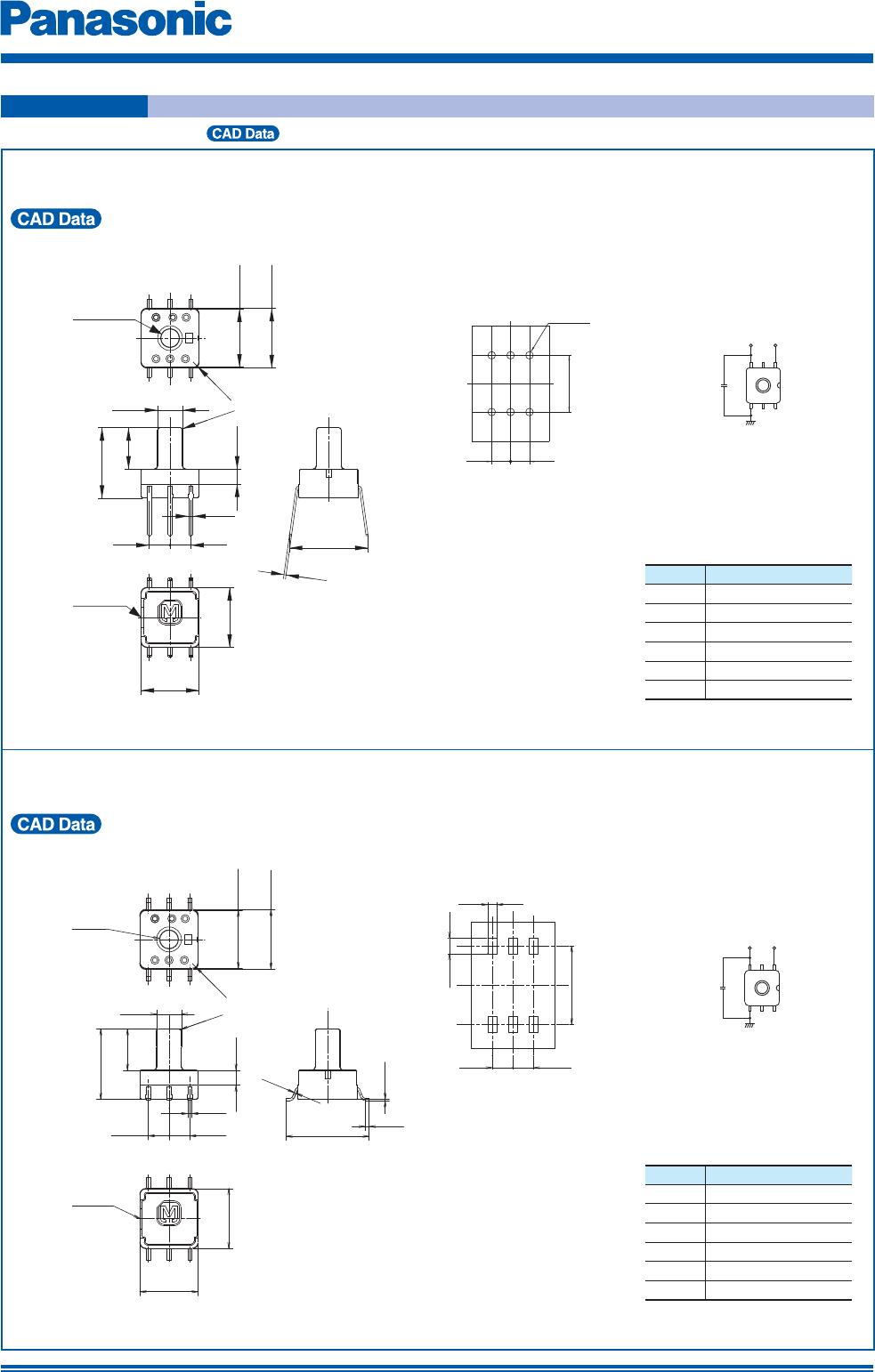
Pressure Sensor/PS-A (ADP5)
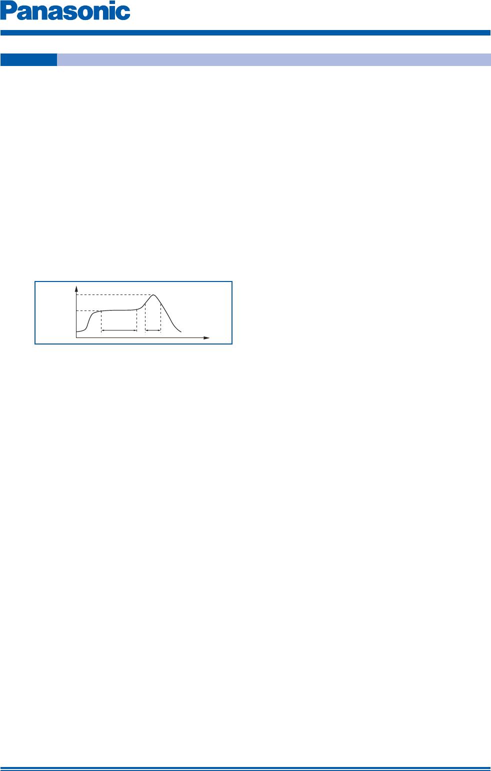
Preheating
With in 60 sec.
With in
10 sec.
230 °C
150 °C
446 °F
302 °F
Main heating
Temperature
Time
NOTES
■ Mounting
Use the land of the printed-circuit board on which the sensor is
securely fixed.
■ Soldering
Avoid the external thermal influence as the product has a limited
thermal capacity due to its compact structure. Heat deformation
may damage the sensor or deteriorate its performance. Use the
non-corrosive rosin flux. Prevent the flux from entering into the
inside of the product as the sensor is exposed to the atmosphere.
1) Manual soldering
• Raise the temperature of the soldering tip between 260 and
300 °C
500 and 572 °F (30 W) and solder within 5 seconds.
• The sensor output may vary if the load is applied on the
terminal during soldering.
• Keep the soldering tip clean.
2) DIP soldering (DIP Terminal)
• Keep the temperature of the DIP solder tank below 260 °C
572 °F and solder within 5 seconds.
• To avoid heat deformation, do not perform DIP soldering
when mounting on the circuit board which has a small
thermal capacity.
3) Reflow soldering (SMD Terminal)
• The recommended reflow temperature profile conditions are
given below.
• We recommend the screen solder printing method as the
method of cream.
• Please refer to the recommended PC board specification
diagram for the PC board foot pattern.
• Self alignment may not always work as expected, therefore,
please carefully the position of the terminals and pattern.
• The temperature of the profile is assumed to be a value
measured with the printed wiring board of the terminal
neighborhood.
• Please evaluate solderbility under the actual mounting
conditions since welding and deformation of the pressure
inlet port may occur due to heat stress depending on
equipments or conditions.
4) Rework soldering
• Complete rework at a time.
• Use a flattened soldering tip when performing rework on the
solder bridge. Do not add the flux.
• Keep the soldering tip below the temperature described in
the specifications.
5) Avoid drop and rough handling as excessive force may deform
the terminal and damage soldering characteristics.
6) Keep the circuit board warpage within 0.05 mm of the full width
of the sensor.
7) After soldering, do not apply stress on the soldered part when
cutting or bending the circuit board.
8) Prevent human hands or metal pieces from contacting with the
sensor terminal. Such contact may cause anomalous outlets as
the terminal is exposed to the atmosphere.
9) After soldering, prevent chemical agents from adhering to the
sensor when applying coating to avoid insulation deterioration of
the circuit board.
10
) Please consult us concerning leadfree soldering.
■ Wire connection
1) Correctly wire as in the connection diagram. Reverse connection
may damage the product and degrade the performance.
2) Do not use idle terminals to prevent damages to the sensor.
■ Cleaning
• Prevent cleaning liquid from entering the inside of the product
as the sensor is exposed to the atmosphere.
• Do not perform ultrasonic cleaning in order to prevent damages
to the product.
■ Environment
1) Avoid use and storage in the corrosive gas (organic solvent,
sulfurous acid and hydrogen sulfide gases) which negatively
affects the product.
2) Install the capacitor on the power supply terminal of the sensor
and stabilize supply voltage to maintain a superimposed noise
resistance. Recommended installation is to arrange 0.1 F and
1,000 pF in parallel. Before use, check the noise resistance and
select/add the optimal capacitor.
3) Use surge absorbers as applying the external surge voltage may
damage the internal circuit.
4) Malfunction may occur near electric noises from static electricity,
lightning, broadcast or amateur radio stations and mobile phones.
5) Avoid use in a place where these products come in contact with
water as the sensor does not have a splash-proof construction.
6) Avoid use in an environment where these products cause dew
condensation. When water attached to the sensor chip freezes,
the sensor output may be fluctuated or damaged.
7) Due to the structure of the pressure sensor chip, the output
varies under light. Do not expose the sensor chip to light when
applying a voltage by using a transparent tube.
8) Do not apply high-frequency oscillation, such as ultrasonic
waves, to the product.
■ Quality check under actual use conditions
These specifications are for individual components. Before use,
carefully check the performance and quality under actual use
conditions to enhance stability.
■ Other precautions
1) The wrong mounting method and the pressure range may invite
the risk of accidents.
2) Only applicable pressure medium is dry air. Avoid use in the
corrosive gas (organic solvent, sulfurous acid and hydrogen
sulfide gases) or other mediums containing moisture or foreign
substances. Such mediums may damage or break the product.
3) The pressure sensor chip is located inside the pressure
introduction port. Do not insert foreign substances, such as
wires, into the port as those substances may damage the chip
and close the port. Do not block the atmosphere introduction
port.
4) Use electric power within the rated power range. Use beyond
the range may damage the product.
5) Follow below instructions as static electricity may damage the
product:
(1) For Storage, short the circuit between terminals by using
conductive substances or wrap the whole chip with
aluminum foil. For storage and transportation, avoid plastic
containers which are easily electrified.
(2) Before use, connect electrified materials on desk and
operators to the ground in order to safely discharge static
electricity.
6) Carefully select and fix tubes, introduction pipes and products
based on the working voltage. Please contact us for any inquires.
7) After mounding the pressure sensor, prevent the potting agent
from entering the pressure and the atmosphere introduction ports
when coating the circuit board. Use the elastic resin as the heated
resin may expand, contract and apply pressure to the sensor. After
coating, carefully check if the sensor can be used.
Aug. 201500