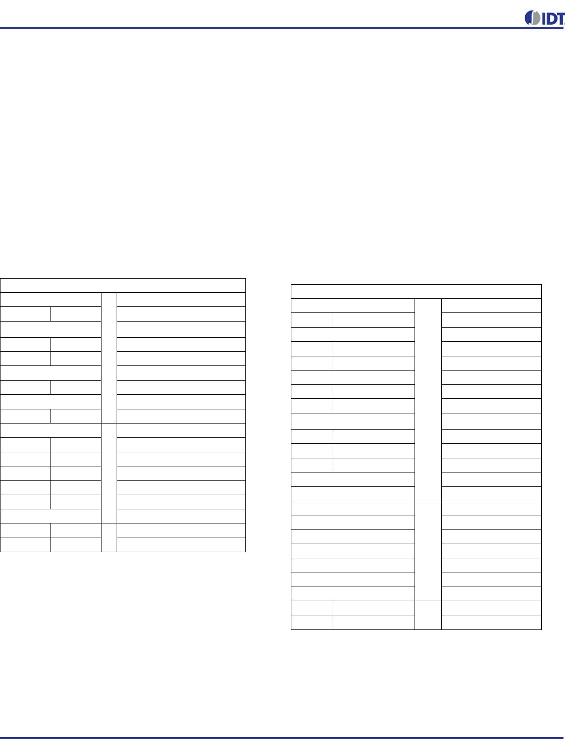
SMBus Table: Output Enable Register
1
Byte 0 Name Control Function Type 0 1 Default
Bit 7
DIF OE5 Output Enable RW Low/Low Enabled 1
Bit 6
DIF OE4 Output Enable RW Low/Low Enabled 1
Bit 5
1
Bit 4
DIF OE3 Output Enable RW Low/Low Enabled 1
Bit 3
DIF OE2 Output Enable RW Low/Low Enabled 1
Bit 2
DIF OE1 Output Enable RW Low/Low Enabled 1
Bit 1
1
Bit 0
DIF OE0 Output Enable RW Low/Low Enabled 1
1. A low on these bits will override the OE# pin and force the differential output Low/Low
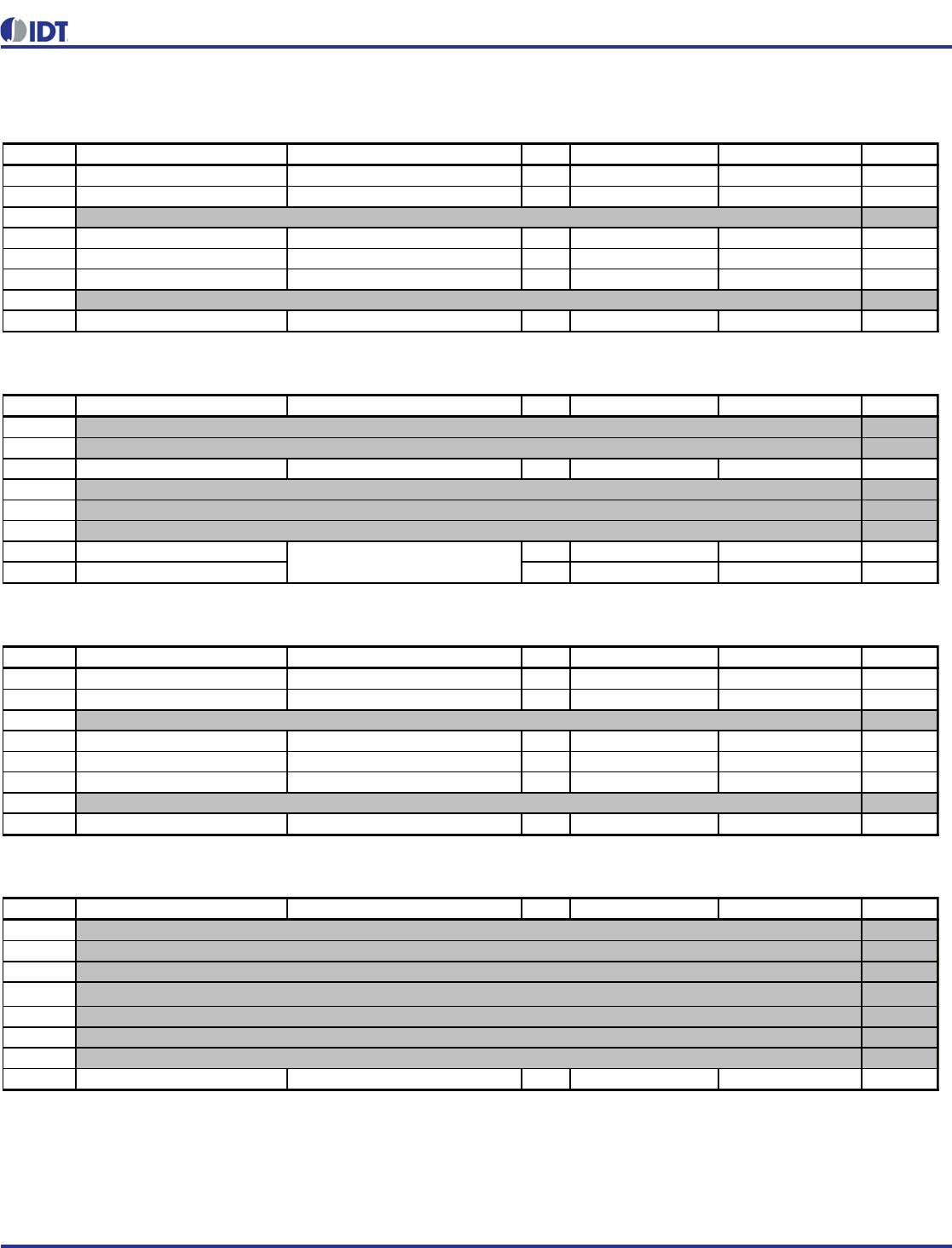
SMBus Table: PLL Operating Mode and Output Amplitude Control Register
Byte 1 Name Control Function Type 0 1 Default
Bit 7
0
Bit 6
1
Bit 5
DIF OE6 Output Enable RW Low/Low Enabled 1
Bit 4
0
Bit 3
1
Bit 2
1
Bit 1
AMPLITUDE 1 RW 00 = 0.55V 01= 0.65V 1
Bit 0
AMPLITUDE 0 RW 10 = 0.7V 11 = 0.8V 0
1. A low on the DIF OE bit will override the OE# pin and force the differential output Low/Low
SMBus Table: DIF Slew Rate Control Register
Byte 2 Name Control Function Type 0 1 Default
Bit 7
SLEWRATESEL DIF5 Adjust Slew Rate of DIF5 RW Slow Setting Fast Setting 1
Bit 6
SLEWRATESEL DIF4 Adjust Slew Rate of DIF4 RW Slow Setting Fast Setting 1
Bit 5
1
Bit 4
SLEWRATESEL DIF3 Adjust Slew Rate of DIF3 RW Slow Setting Fast Setting 1
Bit 3
SLEWRATESEL DIF2 Adjust Slew Rate of DIF2 RW Slow Setting Fast Setting 1
Bit 2
SLEWRATESEL DIF1 Adjust Slew Rate of DIF1 RW Slow Setting Fast Setting 1
Bit 1
1
Bit 0
SLEWRATESEL DIF0 Adjust Slew Rate of DIF0 RW Slow Setting Fast Setting 1
Note: See "DIF 0.7V Low-Power HCSL Outputs" table for slew rates.
SMBus Table: DIF Slew Rate Control Register
Byte 3 Name Control Function Type 0 1 Default
Bit 7
1
Bit 6
1
Bit 5
0
Bit 4
0
Bit 3
0
Bit 2
1
Bit 1
1
Bit 0
SLEWRATESEL DIF6 Adjust Slew Rate of DIF6 RW Slow Setting Fast Setting 1
Note: See "DIF 0.7V Low-Power HCSL Outputs" table for slew rates.
Byte 4 is Reserved and reads back 'hFF
Reserved
Reserved
Reserved
Reserved
Reserved
Controls Output Amplitude
Reserved
Reserved
Reserved
Reserved
Reserved
Reserved
Reserved
Reserved
Reserved
Reserved
Reserved