2002-2012 Microchip Technology Inc. DS21421E-page 1
TC4423/TC4424/TC4425
Features
• High Peak Output Current: 3A
• Wide Input Supply Voltage Operating Range:
- 4.5V to 18V
• High Capacitive Load Drive Capability:
- 1800 pF in 25 ns
• Short Delay Times: <40 ns (typ)
• Matched Rise/Fall Times
• Low Supply Current:
- With Logic ‘1’ Input – 3.5 mA (Max)
- With Logic ‘0’ Input – 350 µA (Max)
• Low Output Impedance: 3.5 (typ)
• Latch-Up Protected: Will Withstand 1.5A Reverse
Current
• Logic Input Will Withstand Negative Swing Up To
5V
• ESD Protected: 4 kV
• Pin compatible with the TC1426/TC1427/TC1428,
TC4426/TC4427/TC4428 and TC4426A/
TC4427A/TC4428A devices.
• Space-saving 8-Pin 6x5 DFN Package
Applications
• Switch Mode Power Supplies
• Pulse Transformer Drive
• Line Drivers
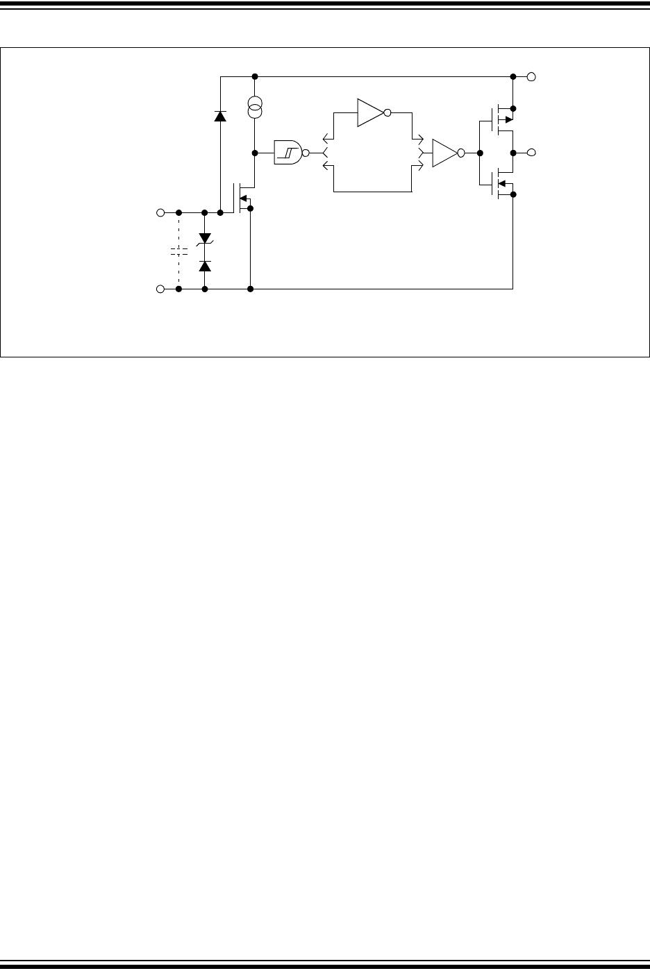
General Description
The TC4423/TC4424/TC4425 devices are a family of
3A, dual-output buffers/MOSFET drivers. Pin compati-
ble with the TC1426/27/28, TC4426/27/28 and
TC4426A/27A/28A dual 1.5A driver families, the
TC4423/24/25 family has an increased latch-up current
rating of 1.5A, making them even more robust for
operation in harsh electrical environments.
As MOSFET drivers, the TC4423/TC4424/TC4425 can
easily charge 1800 pF gate capacitance in under
35 nsec, providing low enough impedances in both the
on and off states to ensure the MOSFET's intended
state will not be affected, even by large transients.
The TC4423/TC4424/TC4425 inputs may be driven
directly from either TTL or CMOS (2.4V to 18V). In
addition, the 300 mV of built-in hysteresis provides
noise immunity and allows the device to be driven from
slowly rising or falling waveforms.
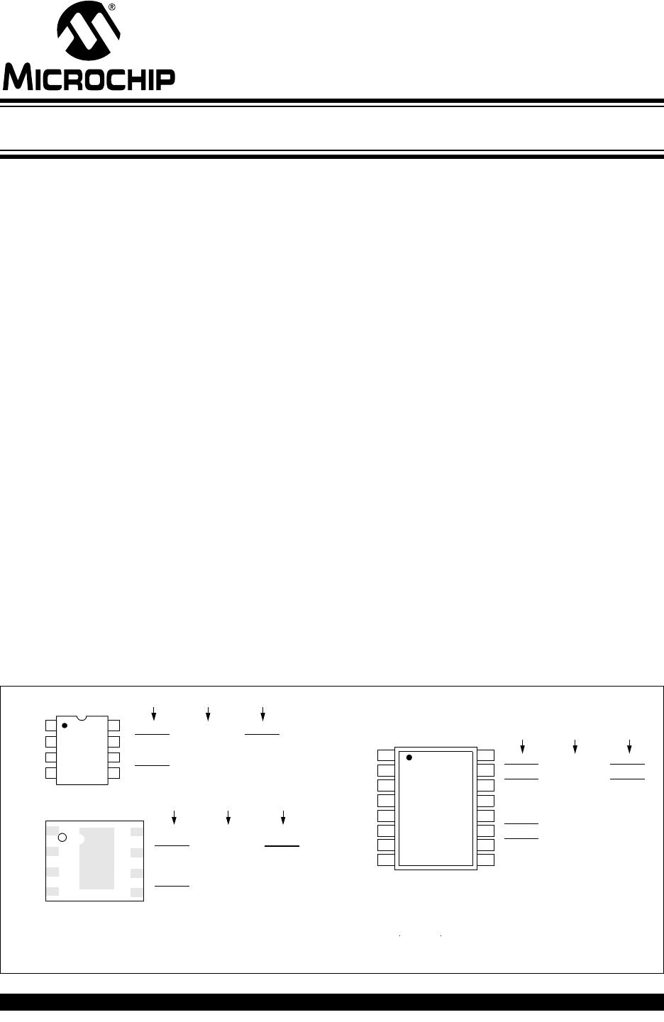
Package Types
(1)
8-Pin DFN
(2)
NC
IN A
GND
IN B
2
3
4
5
6
7
8
1
8-Pin PDIP
1
2
3
4
NC
5
6
7
8
OUT A
OUT B
NC
IN A
GND
IN B
V
DD
TC4423
TC4424
Note 1: Duplicate pins must both be connected for proper operation.
2: Exposed pad of the DFN package is electrically isolated.
TC4423 TC4424
NC
OUT A
OUT B
V
DD
TC4423
TC4424
TC4425
NC
OUT A
OUT B
V
DD
1
2
3
4
5
6
7
8
16
13
12
11
10
9
NC
IN A
NC
GND
GND
NC
IN B
NC
NC
OUT A
V
DD
V
DD
OUT B
OUT B
NC
OUT A
15
14
TC4423
TC4424
TC4425
16-Pin SOIC (Wide)
NC
OUT A
V
DD
V
DD
OUT B
OUT B
NC
OUT A
OUT A
V
DD
V
DD
OUT B
OUT B
NC
OUT A
TC4423 TC4424 TC4425
NC
TC4425
TC4425
NC
OUT A
OUT B
V
DD
TC4423 TC4424
NC
OUT A
OUT B
V
DD
TC4425
NC
OUT A
OUT B
V
DD
3A Dual High-Speed Power MOSFET Drivers