Narrow pitch connectors S35 (0.35mm pitch)
–7–
ACCTB66E 201612-T
NOTES
1. Design of PC board patterns
Conduct the recommended foot pattern design, in order to
preserve the mechanical strength of terminal solder areas.
2. Recommended PC board and metal mask patterns
Connectors are mounted with high pitch density, intervals of 0.35
mm, 0.4 mm or 0.5 mm.
In order to reduce solder and flux rise, solder bridges and other
issues make sure the proper levels of solder is used.
The figures to the right are recommended metal mask patterns.
Please use them as a reference.
• Socket (Mated height: 0.6 mm)
Recommended PC board pattern (TOP VIEW)
Recommended metal mask pattern
Metal mask thickness: When 100μm
(Terminal opening ratio: 70%)
(Metal-part opening ratio: 100%)
• Socket (Mated height: 0.8 mm)
Recommended PC board pattern (TOP VIEW)
Recommended metal mask pattern
Metal mask thickness: When 100μm
(Terminal opening ratio: 70%)
(Metal-part opening ratio: 100%)
• Header (Mated height: 0.6 mm and 0.8 mm)
Recommended PC board pattern (TOP VIEW)
Recommended metal mask pattern
Metal mask thickness: When 100μm
(Terminal opening ratio: 70%)
(Metal-part opening ratio: 100%)
1.64±0.03
0.85±0.03
0.40±0.03
0.49±0.03
0.35±0.03
0.20±0.03
(0.40)
1.35±0.03
0.20±0.03
1.20±0.03
2.00±0.03
: Insulation area
1.35±0.01
0.85±0.01
0.40±0.01
0.49±0.01
2.00±0.01
1.20±0.01
(0.40)
1.64±0.01
(0.22)
0.35±0.01
0.18±0.01
(0.31)
1.38±0.01
2.00±0.01
0.20±0.03
1.20±0.03
0.35±0.03
0.20±0.03
2.00±0.03
(0.40)
0.80±0.03
0.50±0.03
0.40±0.03
1.72±0.03
1.275±0.03
: Insulation area
0.35±0.01
0.18±0.01
(0.31)
1.38±0.01
2.00±0.01
1.72±0.01
1.20±0.01
2.00±0.01
(0.40)
(0.26)
0.40±0.01
0.50±0.01
0.80±0.01
1.28±0.01
: Insulation area
0.35±0.03
1.80±0.03
0.66±0.03
1.00±0.03
1.80±0.03
1.00±0.03
(0.40)
(0.40)
0.20±0.03
0.28±0.03
0.70±0.03
0.35±0.01
1.80±0.01
1.18±0.01
1.80±0.01
1.00±0.01
(0.40)
(0.31)
0.18±0.01
0.28±0.01
0.70±0.01
Please refer to the latest product
specifications when designing your
product.
–1–
ACCTB48E 201606-T
For board-to-board/board-to-FPC
About safety Remarks
Regarding the design of devices and PC board patterns
Regarding the selection of the connector placement machine and the mounting
procedures
Notes on Using Narrow pitch Connectors/
High Current Connectors
1) Do not use these connectors beyond
the specification sheets. The usage
outside of specified rated current,
dielectric strength, and environmental
conditions and so on may cause circuitry
damage via abnormal heating, smoke,
and fire.
2) In order to avoid accidents, your
thorough specification review is
appreciated.
Please contact us if your usage is out of
the specifications. Otherwise, Panasonic
Corporation cannot guarantee the quality
and reliability.
3) Panasonic Corporation is consistently
striving to improve quality and reliability.
However, the fact remains that electrical
components and devices generally cause
failures at a given statistical probability.
Furthermore, their durability varies with
use environments or use conditions. In
this respect, please check for actual
electrical components and devices under
actual conditions before use.
Continued usage in a state of degraded
condition may cause the deteriorated
insulation, thus result in abnormal heat,
smoke or firing. Please carry out safety
design and periodic maintenance
including redundancy design, design for
fire spread prevention, and design for
malfunction prevention so that no
accidents resulting in injury or death, fire
accidents, or social damage will be
caused as a result of failure of the
products or ending life of the products.
1) When using the board to board
connectors, do not connect a pair of
board with multiple connectors.
Otherwise, misaligned connector
positions may cause mating failure or
product breakage.
2) With mounting equipment, there may
be up to a ±0.2 to 0.3-mm error in
positioning. Be sure to design PC boards
and patterns while taking into
consideration the performance and
abilities of the required equipment.
3) Some connectors have tabs embossed
on the body to aid in positioning. When
using these connectors, make sure that
the PC board is designed with positioning
holes to match these tabs.
4) To ensure the required mechanical
strength when soldering the connector
terminals, make sure the PC board
meets recommended PC board pattern
design dimensions given.
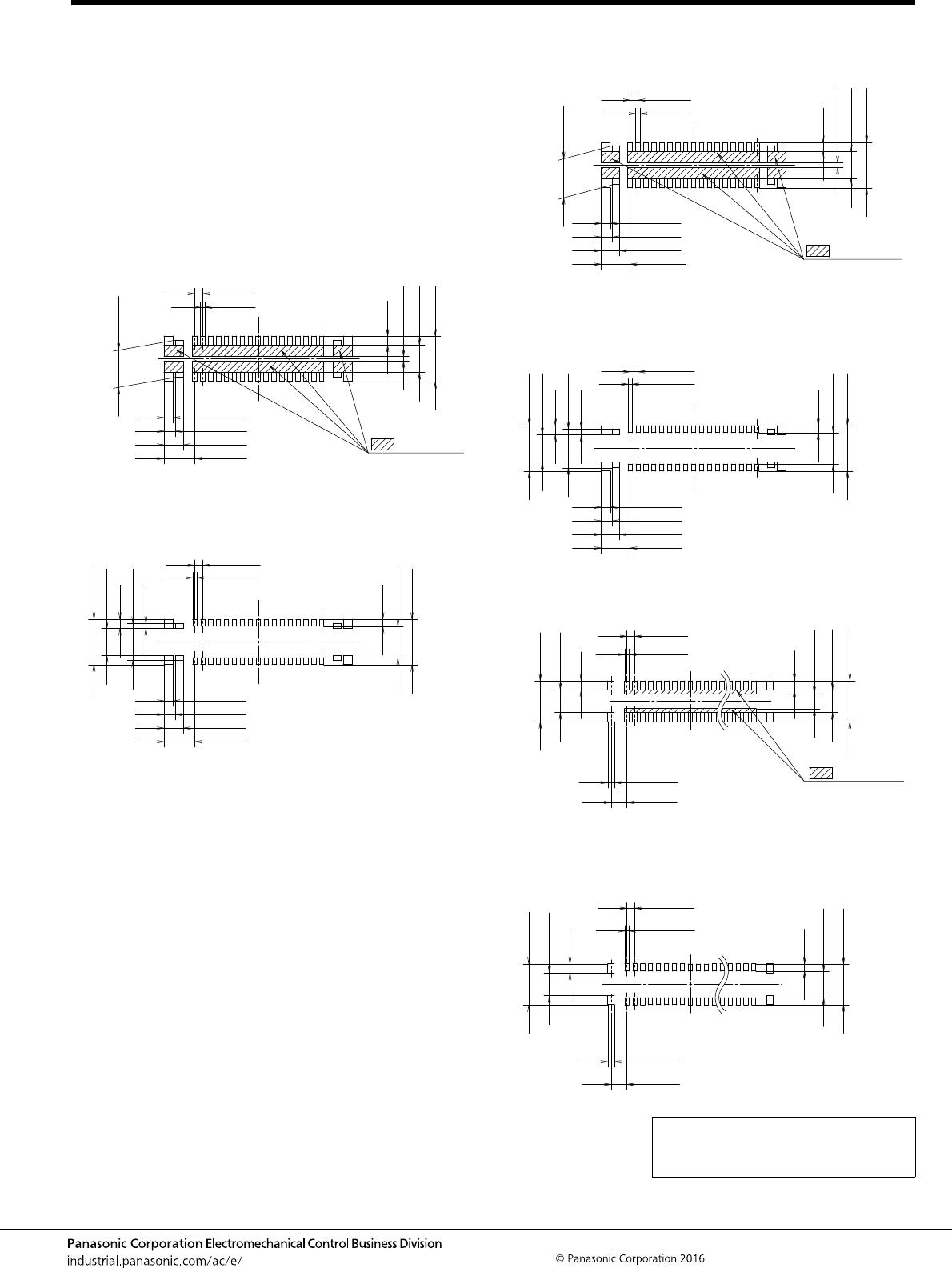
5) PC board
Control the thicknesses of the coverlay
and adhesive to prevent poor soldering.
This connector has no stand-off.
Therefore, minimize the thickness of the
coverlay, etc. so as to prevent the
occurrence of poor soldering.
6) For all connectors of the narrow pitch
series, to prevent the PC board from
coming off during vibrations or impacts,
and to prevent loads from falling directly
on the soldered portions, be sure to
design some means to fix the PC board
in place.
Example) Secure in place with screws
When connecting PC boards, take
appropriate measures to prevent the
connector from coming off.
7) When mounting connectors on a FPC
board:
When the connector soldered to FPC is
mated or unmated, solder detachment
may occur by the force to the terminals.
Connector handling is recommended in
the condition when the reinforcing plate is
attached to the backside of FPC where
the connector is mounted. The external
dimension of the reinforcing plate is
recommended to be larger than the
dimension of “PC board recommended
process pattern” (extended dimension of
one side is approximately 0.5 to 1.0 mm).
The materials and thickness of the
reinforcing plate are glass epoxy or
polyimide (thickness 0.2 - 0.3 mm) or
SUS (thickness 0.1 - 0.2 mm).
• As this connector has temporary locking
structure, the connector mating may be
separated by the dropping impact
depend on the size, weight or bending
force of the FPC. Please consider the
measures at usage to prevent the mating
separation.
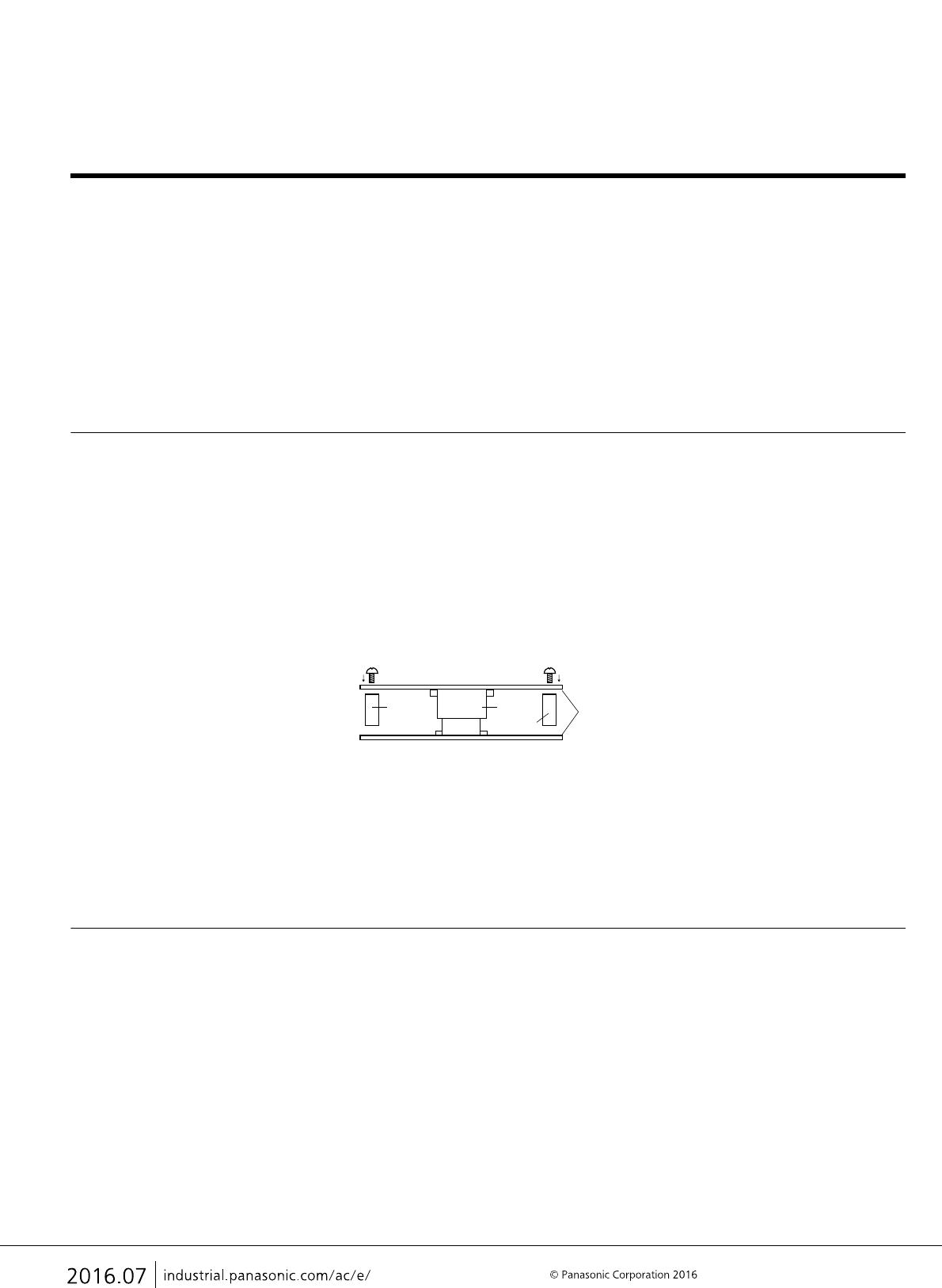
8) The narrow pitch connector series is
designed to be compact and thin.
Although ease of handling has been
taken into account, take care when
mating the connectors, as displacement
or angled mating could damage or
deform the connector.
Connector
Spacer
Spacer
PC board
Screw
1) Select the placement machine taking
into consideration the connector height,
required positioning accuracy, and
packaging conditions.
2) Be aware that if the chucking force of
the placement machine is too great, it
may deform the shape of the connector
body or connector terminals.
3) Be aware that during mounting,
external forces may be applied to the
connector contact surfaces and terminals
and cause deformations.
4) Depending on the size of the
connector being used, self alignment
may not be possible. In such cases, be
sure to carefully position the terminal with
the PC board pattern.
5) The positioning bosses give an
approximate alignment for positioning on
the PC board. For accurate positioning of
the connector when mounting it to the PC
board, we recommend using an
automatic positioning machine.
6) In case of dry condition, please note
the occurrence of static electricity.
The product may be adhered to the
embossed carrier tape or the cover tape
in dry condition.
Recommended humidity is from 40%RH
to 60%RH and please remove static
electricity by ionizer in manufacturing
process.
Notes on Using Narrow pitch Connectors/High Current Connectors
–2–
ACCTB48E 201606-T
Regarding soldering
Handling Single Components
Precautions for mating
Reflow soldering
1) Measure the recommended profile
temperature for reflow soldering by
placing a sensor on the PC board near
the connector surface or terminals.
(Please refer to the specification for detail
because the temperature setting differs
by products.)
2) As for cream solder printing, screen
printing is recommended.
3) When setting the screen opening area
and PC board foot pattern area, refer the
recommended PC board pattern and
window size of metal mask on the
specification sheet, and make sure that
the size of board pattern and metal mask
at the base of the terminals are not
increased.
4) Please pay attentions not to provide
too much solder. It makes miss mating
because of interference at soldering
portion when mating.
5) When mounting on both sides of the
PC board and the connector is mounting
on the underside, use adhesives or other
means to ensure the connector is
properly fixed to the PC board. (Double
reflow soldering on the same side is
possible.)
6) The condition of solder or flux rise and
wettability varies depending on the type
of solder and flux. Solder and flux
characteristics should be taken into
consideration and also set the reflow
temperature and oxygen level.
7) Do not use resin-containing solder.
Otherwise, the contacts might be firmly
fixed.
8) Soldering conditions
Please use the reflow temperature profile
conditions recommended below for
reflow soldering. Please contact us
before using a temperature profile other
than that described below (e.g. lead-free
solder).
For products other than the ones above,
please refer to the latest product
specifications.
9) The temperature profiles given in this
catalog are values measured when using
the connector on a resin-based PC
board. When performed reflow soldering
on a metal board (iron, aluminum, etc.) or
a metal table to mount on a FPC, make
sure there is no deformation or
discoloration of the connector before
mounting.
10) Consult us when using a screen-
printing thickness other than that
recommended.
Hand soldering
1) Set the soldering iron so that the tip
temperature is less than that given in the
table below.
Table A
2) Do not allow flux to spread onto the
connector leads or PC board. This may
lead to flux rising up to the connector
inside.
3) Touch the soldering iron to the foot
pattern. After the foot pattern and
connector terminal are heated, apply the
solder wire so it melts at the end of the
connector terminals.
4) Be aware that soldering while applying
a load on the connector terminals may
cause improper operation of the
connector.
5) Thoroughly clean the soldering iron.
6) Flux from the solder wire may get on
the contact surfaces during soldering
operations. After soldering, carefully
check the contact surfaces and clean off
any solder before use.
7) These connector is low profile type. If
too much solder is supplied for hand
soldering, It makes miss mating because
of interference at soldering portion.
Please pay attentions.
Solder reworking
1) Finish reworking in one operation.
2) In case of soldering rework of bridges.
Don’t use supplementary solder flux.
Doing so may cause contact problems by
flux.
3) Keep the soldering iron tip temperature
below the temperature given in Table A.
Terminal
Paste
solder
PC board
foot pattern
Product name Soldering iron temperature
SMD type connectors
300°C within 5 sec.
350°C within 3 sec.
60 to 120 sec.
Preheating
Peak temperature
200°C
220°C
Upper limited (Solder heat resistance)
Peak temperature 260°C
230°C
180°C
150°C
70 sec.
25 sec.
Lower limited (Solder wettability)
Time
Temperature
Apply the solder
wire here
Terminal
Pattern
PC board
Small angle as
possible up to
45 degrees
Soldering
iron
1) Make sure not to drop or allow parts to
fall from work bench.
2) Excessive force applied to the
terminals could cause warping, come
out, or weaken the adhesive strength of
the solder. Handle with care.
3) Do not insert or remove the connector
when it is not soldered. Forcibly applied
external pressure on the terminals can
weaken the adherence of the terminals to
the molded part or cause the terminals to
lose their evenness.
This product is designed with ease of
handling. However, in order to prevent the
deformation or damage of contacts and
molding, take care and do not mate the
connectors as shown right.
Strongly pressed and twisted
Tilted mating
Press-fitting while the mating
inlets of the socket and
header are not matched.

AXG130144A

Mfr. #:
Manufacturer:
Panasonic
Description:
CONN SOCKET 30POS SMD GOLD
Lifecycle:
New from this manufacturer.
Delivery:
DHL FedEx Ups TNT EMS
Payment:
T/T Paypal Visa MoneyGram Western Union