XCR3128XL-7TQ144C

DS016 (v2.6) March 31, 2006 www.xilinx.com 1
Product Specification
© 2006 Xilinx, Inc. All rights reserved. All Xilinx trademarks, registered trademarks, patents, and disclaimers are as listed at http://www.xilinx.com/legal.htm.
All other trademarks and registered trademarks are the property of their respective owners. All specifications are subject to change without notice.
Features
Low power 3.3V 128 macrocell CPLD
5.5 ns pin-to-pin logic delays
System frequencies up to 175 MHz
128 macrocells with 3,000 usable gates
Available in small footprint packages
- 144-pin TQFP (108 user I/O pins)
- 144-ball CS BGA (108 user I/O)
- 100-pin VQFP (84 user I/O)
Optimized for 3.3V systems
- Ultra low power operation
- Typical Standby Current of 17 μA at 25°
C
- 5V tolerant I/O pins with 3.3V core supply
- Advanced 0.35 micron five layer metal EEPROM
process
- Fast Zero Power™ (FZP) CMOS design
technology
- 3.3V PCI electrical specification compatible outputs
(no internal clamp diode on any input or I/O)
Advanced system features
- In-system programming
- Input registers
- Predictable timing model
- Up to 23 available clocks per function block
- Excellent pin retention during design changes
- Full IEEE Standard 1149.1 boundary-scan (JTAG)
- Four global clocks
- Eight product term control terms per function block
Fast ISP programming times
Port Enable pin for additional I/O
2.7V to 3.6V supply voltage at industrial temperature
range
Programmable slew rate control per output
Security bit prevents unauthorized access
Refer to XPLA3 family data sheet (DS012
) for
architecture description
Description
The CoolRunner™ XPLA3 XCR3128XL device is a 3.3V
128 macrocell CPLD targeted at power sensitive designs
that require leading edge programmable logic solutions. A
total of eight function blocks provide 3,000 usable gates.
Pin-to-pin propagation delays are as fast as 5.5 ns with a
maximum system frequency of 175 MHz.
TotalCMOS Design Technique for Fast
Zero Power
CoolRunner XPLA3 CPLDs offer a TotalCMOS™ solution,
both in process technology and design technique. Xilinx
employs a cascade of CMOS gates to implement its sum of
products instead of the traditional sense amp approach.
This CMOS gate implementation allows Xilinx CPLDs to
offer devices that are both high performance and low power,
breaking the paradigm that to have low power, you must
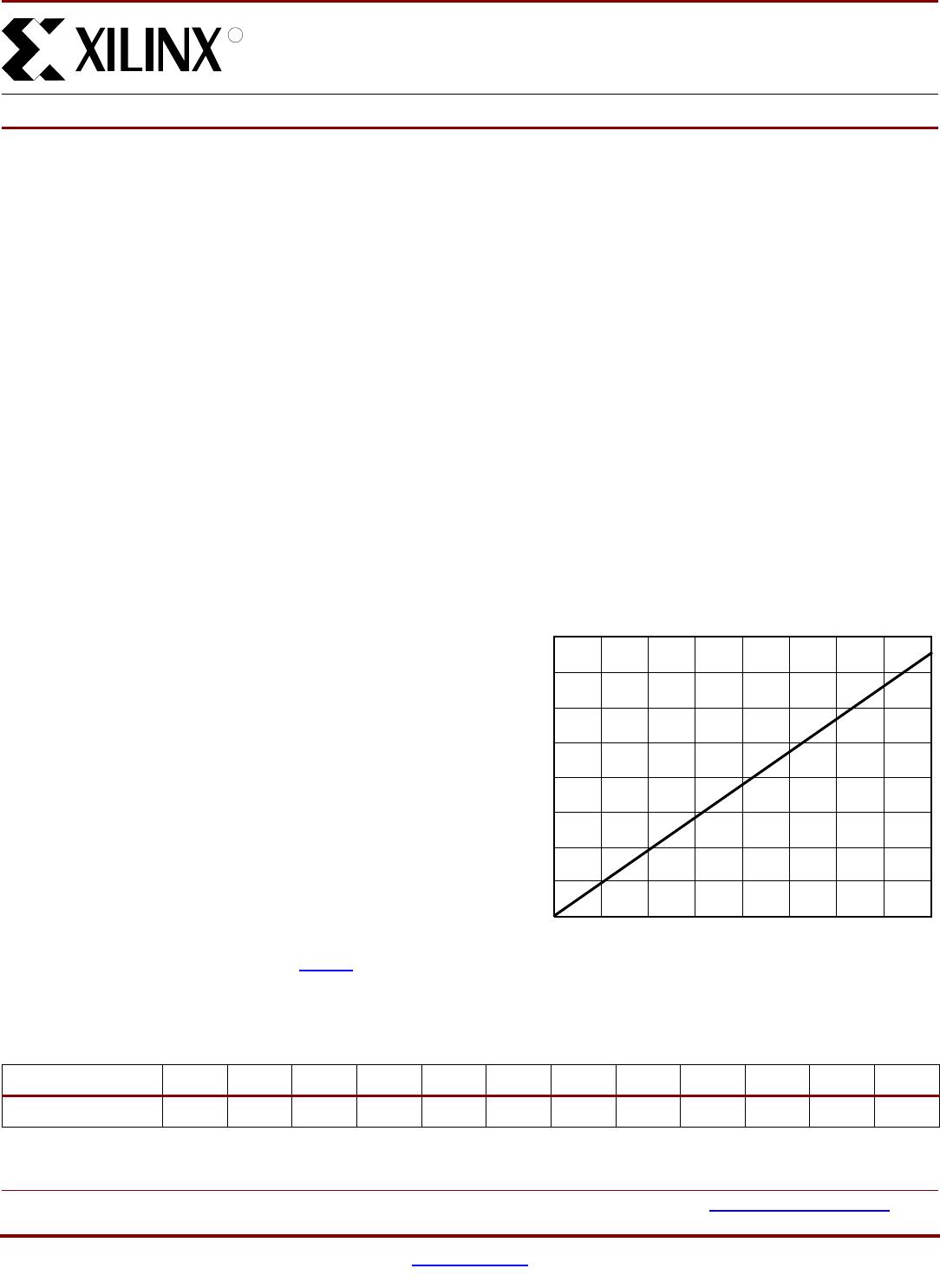
have low performance. Refer to Figure 1 or Figure 2 and
Table 1or Ta ble 2 showing the I
CC
vs. Frequency of the
XCR3128XL TotalCMOS CPLD (data taken with eight
resetable up/down, 16-bit counters at 3.3V, 25°C).
0
XCR3128XL 128 Macrocell CPLD
DS016 (v2.6) March 31, 2006
014
Product Specification
R
Figure 1: Typical I
CC
vs. Frequency at V
CC
= 3.3V, 25°C
Frequency (MHz)
DS016_01_120902
Typical I
CC
(mA)
0
0
10
20
30
50
70
80
40
60
120 140 16010080604020
Table 1: Typical I
CC
vs. Frequency at V
CC
= 3.3V, 25°C
Frequency (MHz) 0 1 5 10 20 40 60 80 100 120 140 160
Typical I
CC
(mA) 0.017 0.5 2.48 4.97 9.89 19.7 29.5 39.1 48.7 58.0 67.3 76.8
XCR3128XL 128 Macrocell CPLD
2 www.xilinx.com DS016 (v2.6) March 31, 2006
Product Specification
R
DC Electrical Characteristics Over Recommended Operating Conditions
(1)
Symbol Parameter Test Conditions Typical Min. Max. Unit
V
OH
(2)
Output High voltage V
CC
= 3.0V to 3.6V, I
OH
= –8 mA 2.4 - V
V
CC
= 2.7V to 3.0V, I
OH
= –8 mA 2.0 - V
I
OH
= –500 μA 90% V
CC
(3)
-V
V
OL
Output Low voltage for 3.3V outputs I
OL
= 8 mA - 0.4 V
I
IL
Input leakage current V
IN
= GND or V
CC
to 5.5V –10 10 μA
I
IH
I/O High-Z leakage current V
IN
= GND or V
CC
to 5.5V –10 10 μA
I
CCSB
(7)
Standby current V
CC
= 3.6V 29 - 100 μA
I
CC
Dynamic current
(4,5)
f = 1 MHz - 1 mA
f = 50 MHz - 30 mA
C
IN
Input pin capacitance
(6)
f = 1 MHz - 8 pF
C
CLK
Clock input capacitance
(6)
f = 1 MHz - 12 pF
C
I/O
I/O pin capacitance
(6)
f = 1 MHz - 10 pF
Notes:
1. See the CoolRunner XPLA3 family data sheet (
DS012) for recommended operating conditions.
2. See Figure 2 for output drive characteristics of the XPLA3 family.
3. This parameter guaranteed by design and characterization, not by testing.
4. See Tabl e 1, Figure 1 for typical values.
5. This parameter measured with a 16-bit, resetable up/down counter loaded into every function block, with all outputs disabled and
unloaded. Inputs are tied to V
CC
or ground. This parameter guaranteed by design and characterization, not testing.
6. Typical values, not tested.
7. Typical value at 70° C.
Figure 2: Typical I/V Curve for the CoolRunner XPLA3 Family, 25°C
0
0
1
0
2
0
30
4
0
50
7
0
90
1
00
0
.
5
1
1.
5
2
2.
5
3
3
.
5
4
4.
5
5
Volt
s
I
O
L
(
3.3V
)
I
O
H
(
3.3V
)
I
O
H
(
2.7V
)
mA
DS012
_
10
_
03180
2
XCR3128XL 128 Macrocell CPLD
DS016 (v2.6) March 31, 2006 www.xilinx.com 3
Product Specification
R
AC Electrical Characteristics Over Recommended Operating Conditions
(1,2)
Internal Timing Parameters
(1,2)
Symbol Parameter
-6 -7 -10
Unit Min. Max. Min. Max. Min. Max.
T
PD1
Propagation delay time (single p-term) - 5.5 - 7.0 - 9.1 ns
T
PD2
Propagation delay time (OR array)
(3)
- 6.0 - 7.5 - 10.0 ns
T
CO
Clock to output (global synchronous pin clock) - 4.0 5.0 - 6.5 ns
T
SUF
Setup time (fast input register) 2.5 - 3.0 - 3.0 - ns
T
SU1
(4)
Setup time (single p-term) 3.5 - 4.3 - 5.4 - ns
T
SU2
Setup time (OR array) 4.0 - 4.8 - 6.3 - ns
T
H
(4)
Hold time 0 - 0 - 0 - ns
T
WLH
(4)
Global Clock pulse width (High or Low) 2.5 - 3.0 - 4.0 - ns
T
PLH
(4)
P-term clock pulse width 4.0 - 5.0 - 6.0 - ns
T
APRPW
Asynchronous preset/reset pulse width (High or Low) 4.0 - 5.0 - 6.0 - ns
T
R
(4)
Input rise time - 20 - 20 - 20 ns
T
L
(4)
Input fall time - 20 - 20 - 20 ns
f
SYSTEM
(4)
Maximum system frequency - 175 - 119 - 95 MHz
T
CONFIG
(4)
Configuration time
(5)
- 100 - 100 - 100 μs
T
INIT
(4)
ISP initialization time - 100 - 100 - 100 μs
T
POE
(4)
P-term OE to output enabled - 7.5 - 9.3 - 11.2 ns
T
POD
(4)
P-term OE to output disabled
(6)
- 7.5 - 9.3 - 11.2 ns
T
PCO
(4)
P-term clock to output - 7.0 - 8.3 - 10.7 ns
T
PAO
(4)
P-term set/reset to output valid - 8.0 - 9.3 - 11.2 ns
Notes:
1. Specifications measured with one output switching.
2. See the CoolRunner XPLA3 family data sheet (DS012) for recommended operating conditions.
3. See Figure 6 for derating.
4. These parameters guaranteed by design and/or characterization, not testing.
5. Typical current draw during configuration is 9 mA at 3.6V.
6. Output C
L
= 5 pF.
Symbol Parameter
-6 -7 -10
UnitMin. Max. Min. Max. Min. Max.
Buffer Delays
T
IN
Input buffer delay - 1.3 - 1.6 - 2.2 ns
T
FIN
Fast Input buffer delay - 2.3 - 3.0 - 3.1 ns
T
GCK
Global Clock buffer delay - 0.8 - 1.0 - 1.3 ns
T
OUT
Output buffer delay - 2.2 - 2.7 - 3.6 ns
T
EN
Output buffer enable/disable delay - 4.2 - 5.0 - 5.7 ns
Internal Register and Combinatorial Delays
T
LDI
Latch transparent delay - 1.3 - 1.6 - 2.0 ns
T
SUI
Register setup time 1.0 - 1.0 - 1.2 - ns
T
HI
Register hold time 0.3 - 0.5 - 0.7 - ns

XCR3128XL-7TQ144C

Mfr. #:
Manufacturer:
Xilinx
Description:
CPLD - Complex Programmable Logic Devices XCR3128XL-7TQ144C
Lifecycle:
New from this manufacturer.
Delivery:
DHL FedEx Ups TNT EMS
Payment:
T/T Paypal Visa MoneyGram Western Union