_______________General Description
The MAX531/MAX538/MAX539 are low-power, voltage-
output, 12-bit digital-to-analog converters (DACs) speci-
fied for single +5V power-supply operation. The MAX531
can also be operated with ±5V supplies. The
MAX538/MAX539 draw only 140µA, and the MAX531
(with internal reference) draws only 260µA. The
MAX538/MAX539 come in 8-pin DIP and SO packages,
while the MAX531 comes in 14-pin DIP and SO pack-
ages. All parts have been trimmed for offset voltage,
gain, and linearity, so no further adjustment is necessary.
The MAX538’s buffer is fixed at a gain of +1 and the
MAX539’s buffer at a gain of +2. The MAX531’s internal
op amp may be configured for a gain of +1 or +2, as
well as for unipolar or bipolar output voltages. The
MAX531 can also be used as a four-quadrant multiplier
without external resistors or op amps.
For parallel data inputs, see the MAX530 data sheet.
_______________________Applications
Battery-Powered Test Instruments
Digital Offset and Gain Adjustment
Battery-Operated/Remote Industrial Controls
Machine and Motion Control Devices
Cellular Telephones
___________________________Features
♦ Operate from Single +5V Supply
♦ Buffered Voltage Output
♦ Internal 2.048V Reference (MAX531)
♦ 140µA Supply Current (MAX538/MAX539)
♦ INL = ±1/2LSB (max)
♦ Guaranteed Monotonic over Temperature
♦ Flexible Output Ranges:
0V to V
DD
(MAX531/MAX539)
V
SS
to V
DD
(MAX531)
0V to 2.6V (MAX531/MAX538)
♦ 8-Pin SO/DIP (MAX538/MAX539)
♦ Power-On Reset
♦ Serial Data Output for Daisy-Chaining
______________Ordering Information
MAX531/MAX538/MAX539
+5V, Low-Power, Voltage-Output,
Serial 12-Bit DACs
________________________________________________________________
Maxim Integrated Products
1
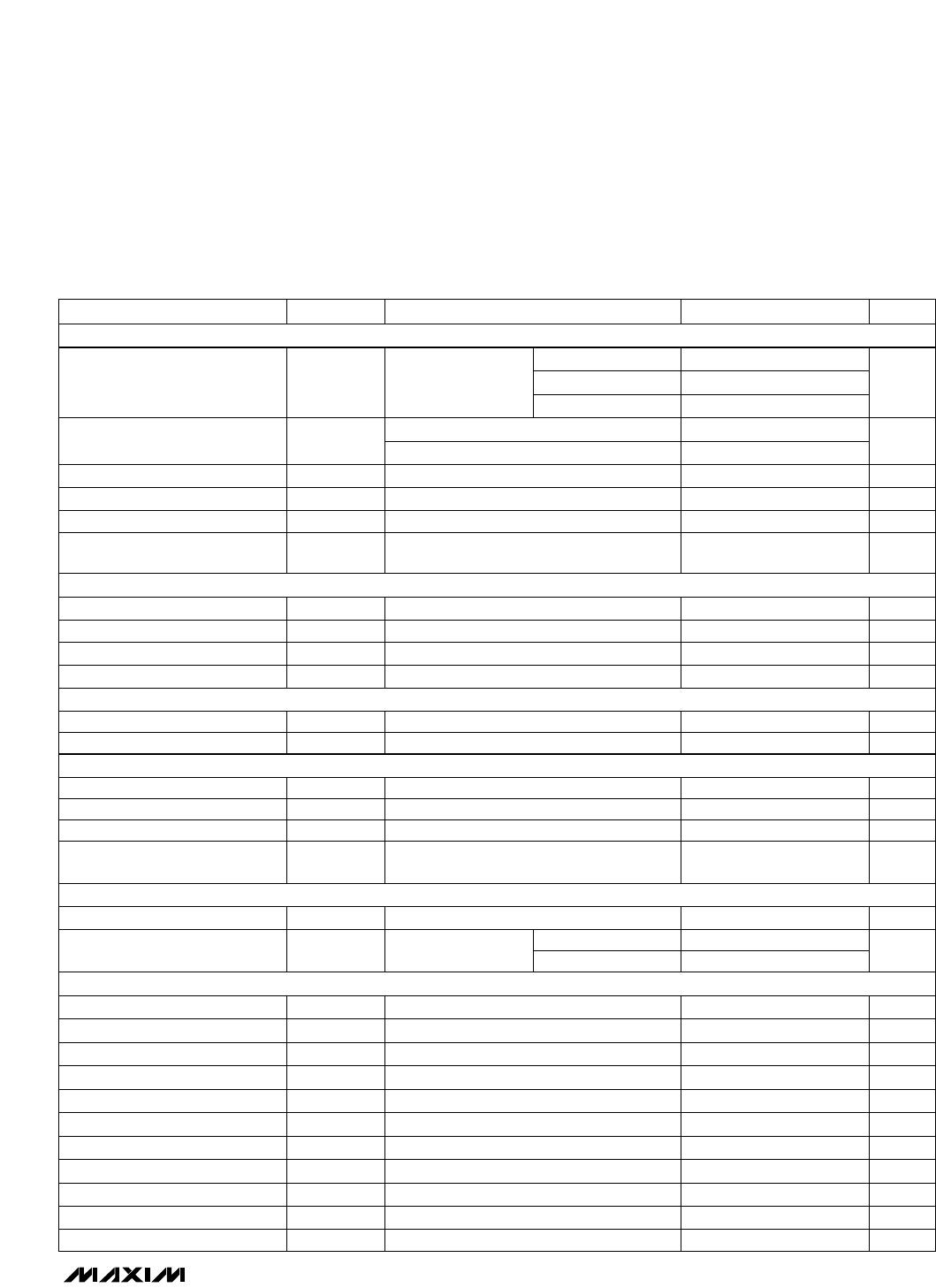
1
2
3
4
8
7
6
5
V
DD
VOUT
REFIN
AGND
DOUT
CS
SCLK
DIN
DIP/SO
TOP VIEW
MAX538
MAX539
_________________Pin Configurations
________________Functional Diagram
For free samples & the latest literature: http://www.maxim-ic.com, or phone 1-800-998-8800
19-0172; Rev 6; 2/97
PART TEMP. RANGE PIN-PACKAGE
MAX531ACPD
0°C to +70°C 14 Plastic DIP
MAX531BCPD 0°C to +70°C 14 Plastic DIP
MAX531ACSD 0°C to +70°C 14 SO
MAX531BCSD 0°C to +70°C 14 SO
ERROR
(LSB)
±1/2
±1
±1/2
±1
DAC
DAC REGISTER
(12 BITS)
SHIFT REGISTER
(12 BITS)
4
BITS
CONTROL
LOGIC
POWER-UP
RESET
2.048V
REFERENCE
(MAX531 ONLY)
AGND
SCLK
DIN
(MAX531 ONLY)
REFOUT
REFIN
(MAX531 ONLY)
BIPOFF
RFB
(MAX531
ONLY)
VOUT
V
DD
DGND
(MAX531
ONLY)
V
SS
(MAX531
ONLY)
DOUT
(LSB)
(MSB)
CLR
(MAX531
ONLY)
CS
MAX531
MAX538
MAX539
MAX531BC/D 0°C to +70°C Dice* ±1
Ordering Information continued at end of data sheet.
*Dice are specified at T
A
= +25°C only.
Pin Configurations continued at end of data sheet.