OP249 Data Sheet
Rev. I | Page 6 of 18
ABSOLUTE MAXIMUM RATINGS
Table 5.
Parameter
1
Rating
Supply Voltage ±18 V
Input Voltage
2
±18 V
Differential Input Voltage
2
36 V
Output Short-Circuit Duration Indefinite
Storage Temperature Range 65°C to +175°C
Operating Temperature Range
OP249A (Q) 55°C to +125°C
OP249F (Q)
40°C to +85°C
OP249G (N, R) 40°C to +85°C
Junction Temperature Range
OP249A (Q), OP249F (Q) 65°C to +175°C
OP249G (N, R) 65°C to +150°C
Lead Temperature (Soldering, 60 sec)
300°C
1
Absolute maximum ratings apply to packaged parts, unless otherwise noted.
2
For supply voltages less than ±18 V, the absolute maximum input voltage is
equal to the supply voltage.
Stresses at or above those listed under Absolute Maximum
Ratings may cause permanent damage to the product. This is a
stress rating only; functional operation of the product at these
or any other conditions above those indicated in the operational
section of this specification is not implied. Operation beyond
the maximum operating conditions for extended periods may
affect product reliability.
Table 6. Thermal Resistance
Package Type θ
JA
1
θ
JC
Unit
8-Lead CERDIP (Q) 134 12 °C/W
8-Lead PDIP (N) 96 37 °C/W
8-Lead SOIC (R) 150 41 °C/W
1
θ
JA
is specified for worst-case mounting conditions, that is, θ
JA
is specified for
device in socket for CERDIP and PDIP packages; θ
JA
is specified for device
soldered to printed circuit board for SOIC package.
ESD CAUTION
Data Sheet OP249
Rev. I | Page 7 of 18
TYPICAL PERFORMANCE CHARACTERISTICS
120
100
80
60
40
20
0
–20
0
45
90
135
180
225
T
A
= 25°C
V
S
= ±15V
R
L
= 2kΩ
FREQUENCY (Hz)
OPEN-LOOP GAIN (dB)
PHASE (°C)
1k
10k
100k 1M 10M 100M
GAIN
PHASE
Θm = 55
00296-006
Figure 6. Open-Loop Gain, Phase vs. Frequency
65
60
45
55
50
10
8
2
6
4
PHASE MARGIN (°C)
V
S
= ±15V
TEMPERATURE (°C)
–75 –50 –25 0 25
50 75 100 125
GAIN BANDWIDTH PRODUCT (MHz)
GBW
Θm
00296-007
Figure 7. Phase Margin, Gain Bandwidth Product vs. Temperature
140
120
100
80
60
40
20
0
FREQUENCY (Hz)
100 1k 10k 100k 1M 10M
T
A
= 25°C
V
S
= ±15V
COMMON-MODE REJECTION (dB)
00296-008
Figure 8. Common-Mode Rejection vs. Frequency
120
100
80
60
40
20
0
T
A
= 25°C
V
S
= ±15V
+PSRR
–PSRR
POWER SUPPLY REJECTION (dB)
FREQUENCY (Hz)
10 100 1k
10k
100k
1M
00296-009
Figure 9. Power Supply Rejection vs. Frequency
28
26
24
–SR
22
20
18
16
TEMPERATURE (°C)
–75 –50 –25 0 25 50 75 100 125
+SR
SLEW RATE (V/µs)
V
S
= ±15V
R
L
= 2kΩ
C
L
= 50pF
00296-010
Figure 10. Slew Rate vs. Temperature
28
26
24
22
20
18
16
DIFFERENTIAL INPUT VOLTAGE (V)
0 0.2 0.4 0.6 0.8 1.0
SLEW RATE (V/µs)
T
A
= 25°C
V
S
= ±15V
R
L
= 2kΩ
00296-011
Figure 11. Slew Rate vs. Differential Input Voltage
OP249 Data Sheet
Rev. I | Page 8 of 18
35
30
25
20
15
10
5
CAPACITIVE LOAD (pF)
0
100
200
300
400
500
SLEW RATE (V/µs)
T
A
= 25°C
V
S
= ±15V
NEGATIVE
POSITIVE
00296-012
Figure 12. Slew Rate vs. Capacitive Load
–10
–8
–6
–4
–2
0
2
4
6
8
10
0.01%
0.01%
0.1%
0.1%
T
A
= 25°C
V
S
= ±15V
A
VCL
= 1
SETTLING TIME (ns)
0 200 400 600 800 1000
OUTPUT STEP SIZE (V)
00296-013
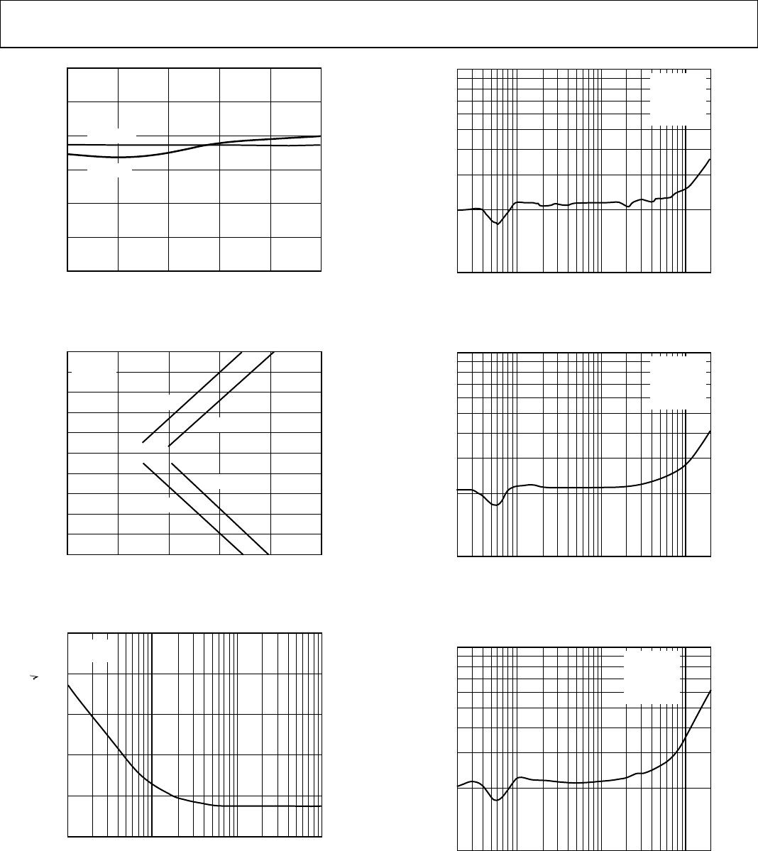
Figure 13. Step Size vs. Settling Time
100
80
60
40
20
0
VOLTAGE NOISE DENSITY (nV/ Hz)
T
A
= 25°C
V
S
= ±15V
FREQUENCY (Hz)
0 100 1k 10k
00296-014
Figure 14. Voltage Noise Density vs. Frequency
0.01
0.001
20 100
1k 10k 20k
T
A
= 25°C
V
S
= ±15V
V
O
= 10V p-p
R
L
= 10kΩ
A
V
= 1
00296-015
Figure 15. Distortion vs. Frequency
0.01
0.001
20 100 1k 10k 20k
T
A
= 25°C
V
S
= ±15V
V
O
= 10V p-p
R
L
= 2kΩ
A
V
= 1
00296-016
Figure 16. Distortion vs. Frequency
0.01
0.001
20 100 1k 10k 20k
T
A
= 25°C
V
S
= ±15V
V
O
= 10V p-p
R
L
= 600Ω
A
V
= 1
00296-017
Figure 17. Distortion vs. Frequency

OP249GS

Mfr. #:
Manufacturer:
Analog Devices Inc.
Description:
Precision Amplifiers DUAL PREC JFET IC High Speed
Lifecycle:
New from this manufacturer.
Delivery:
DHL FedEx Ups TNT EMS
Payment:
T/T Paypal Visa MoneyGram Western Union