Data Sheet OP249
Rev. I | Page 15 of 18
DAC OUTPUT AMPLIFIER
Unity-gain stability, a low offset voltage of 300 µV typical, and a
fast settling time of 870 ns to 0.01%, makes the OP249 an ideal
amplifier for fast DACs.
For CMOS DAC applications, the low offset voltage of the OP249
results in excellent linearity performance. CMOS DACs, such as
the PM7545, typically have a code-dependent output resistance
variation between 11 kΩ and 33 kΩ. The change in output
resistance, in conjunction with the 11 kΩ feedback resistor, results
in a noise gain change, which causes variations in the offset
error, increasing linearity errors. The OP249 features low offset
voltage error, minimizing this effect and maintaining 12-bit
linearity performance over the full-scale range of the converter.
Because the DAC output capacitance appears at the inputs of
the op amp, it is essential that the amplifier be adequately
compensated. Compensation increases the phase margin and
ensures an optimal overall settling response. The required lead
compensation is achieved with Capacitor C in Figure 48.
+15V
PM7545
12
500Ω
75Ω
AGND
DGND
DATA INPUT
REFERENCE
OR V
IN
V
DD
0.1µF
V
OUT
V
DD
R
FB
OUT
1
DB
11
TO DB
0
19
18 20
3
V
REF
C
33pF
–15V
1
2
3
2
8
4
0.1µF
0.1µF
1
1/2
OP249
00296-047
Figure 47. Fast Settling and Low Offset Error of the OP249 Enhances CMOS DAC PerformanceUnipolar Operation
+15V
PM7545
500Ω
75Ω
AGND
DGND
12
DATA INPUT
V
OUT
0.1µF
–15V
1/2
OP249
1/2
OP249
7
5
6
4
R5
10kΩ
1%
R4
20kΩ
1%
R3
10kΩ
1%
1
8
2
3
1
2
3
0.1µF
C
33pF
V
DD
0.1µF
REFERENCE
OR V
IN
DB
11
TO DB
0
OUT
1
R
FB
V
DD
V
REF
18
20
19
00296-048
Figure 48. Fast Settling and Low Offset Error of the OP249 Enhances CMOS DAC PerformanceBipolar Operation
OP249 Data Sheet
Rev. I | Page 16 of 18
10
0%
100
90
500mV 1µs
4µs
10
0%
100
90
500mV 1µs
4µs
A
C = 5pF
RESPONSE IS GROSSLY UNDERDAMPED,
AND EXHIBITS RINGING
B
C = 15pF
FAST RISE TIME CHARACTERISTICS, BUT AT EXPENSE
OF SLIGHT PEAKING IN RESPONSE
00296-049
Figure 49. Effect of Altering Compensation from Circuit in Figure 47PM7545 CMOS DAC with 1/2 OP249, Unipolar Operation;
Critically Damped Response Is Obtained with C ≈ 33 pF
Figure 49 illustrates the effect of altering the compensation on
the output response of the circuit in Figure 47. Compensation is
required to address the combined effect of the output capacitance
of the DAC, the input capacitance of the op amp, and any stray
capacitance. Slight adjustments to the compensation capacitor may
be required to optimize settling response for any given application.
The settling time of the combination of the current output DAC
and the op amp can be approximated by
( ) ( )
22
AMPtDACtTOTALt
SSS
+=
The actual overall settling time is affected by the noise gain of
the amplifier, the applied compensation, and the equivalent
input capacitance at the input of the amplifier.
DISCUSSION ON DRIVING ADCs
Settling characteristics of op amps also include the ability of the
amplifier to recover, that is, settle, from a transient current output
load condition. An example of this includes an op amp driving
the input from a SAR-type ADC. Although the comparison
point of the converter is usually diode clamped, the input swing
of plus-and-minus a diode drop still gives rise to a significant
modulation of input current. If the closed-loop output impedance
is low enough and bandwidth of the amplifier is sufficiently
large, the output settles before the converter makes a comparison
decision, which prevents linearity errors or missing codes.
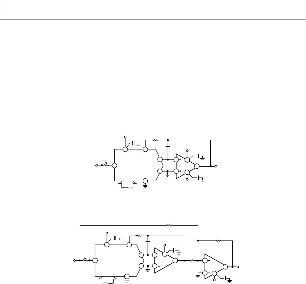
Figure 50 shows a settling measurement circuit for evaluating
recovery from an output current transient. An output disturbing
current generator provides the transient change in output load
current of 1 mA.
+15V
+15V
1.5kΩ
1N4148
220Ω
1.8kΩ
2N3904
1kΩ
*
*
TTL INPUT
+15V
2N2907
7A13 PLUG-IN
7A13 PLUG-IN
300pF
1/2
OP249
+
1kΩ
|V
REF
|
ΔI
OUT
=
–15V
0.1µF
0.1µF
0.1µF
10µF
V
REF
0.01µF
1kΩ
0.47µF
3
2
8
1
4
*DECOUPLE CLOSE TOGETHER ON GROUND
PLANE WITH SHORT LEAD LENGTHS.
00296-050
Figure 50. Transient Output Impedance Test Fixture
As seen in Figure 51, the OP249 has an extremely fast recovery
of 247 ns (to 0.01%) for a 1 mA load transient. The performance
makes it an ideal amplifier for data acquisition systems.
10
0%
100
90
100ns2V2mV
247.4ns
00296-051
Figure 51. Transient Recovery Time of the OP249 from
a 1 mA Load Transient to 0.01%
Data Sheet OP249
Rev. I | Page 17 of 18
OUTLINE DIMENSIONS
COMPLIANT T
O JEDEC STANDARDS MS-001
CONTROLLING DIMENSIONS ARE IN INCHES; MILLIMETER DIMENSIONS
(IN PARENTHESES)
ARE ROUNDED-OFF INCH EQUIVALENTS FOR
REFERENCE ONLY AND ARE NOT
APPROPRIATE FOR USE IN DESIGN.
CORNER LEADS MA
Y BE CONFIGURED AS WHOLE OR HALF LEADS.
070606-
A
0.022 (0.56)
0.018 (0.46)
0.014 (0.36)
SEA
TING
PLANE
0.015
(0.38)
MIN
0.210 (5.33)
MAX
0.150 (3.81)
0.130 (3.30)
0.
1
15 (2.92)
0.070 (1.78)
0.060 (1.52)
0.045 (1.14)
8
1
4
5
0.280 (7.1
1)
0.250 (6.35)
0.240 (6.10)
0.100 (2.54)
BSC
0.400 (10.16)
0.365 (9.27)
0.355 (9.02)
0.060 (1.52)
MAX
0.430 (10.92)
MAX
0.014 (0.36)
0.010 (0.25)
0.008 (0.20)
0.325 (8.26)
0.310 (7.87)
0.300 (7.62)
0.195 (4.95)
0.130 (3.30)
0.1
15 (2.92)
0.015 (0.38)
GAUGE
PLANE
0.005 (0.13)
MIN
Figure 52. 8-Lead Plastic Dual In-Line Package [PDIP]
Narrow Body
(N-8)
Dimensions shown in inches and (millimeters)
CONTROLLING DIMENSIONS ARE IN MILLIMETERS; INCH DIMENSIONS
(IN PARENTHESES) ARE ROUND
ED-OFF MILLIMETER EQUIV
ALENTS FOR
REFERENCE ONLY A
ND ARE NOT APPROPRIATE F
OR USE IN D
ESIGN.
C
OMPLIANT TO JEDEC ST
ANDARDS MS-012-AA
0
124
07-
A
0.25 (
0.0
098)
0.17 (
0.0067)
1.27 (0.0500)
0.40 (0.
0157
)
0.50 (0.0196)
0.
25 (
0.0
099
)
45°
1
.75 (0.0688)
1.3
5 (0
.05
32)
SE
ATIN
G
PL
ANE
0
.25
(0.0098)
0.10 (0.0040)
4
1
8 5
5
.00
(0.1968)
4.80 (0.1890)
4.00 (0.1574)
3
.80 (
0.1
497
)
1.2
7 (0.0500)
B
SC
6.20 (0.2441)
5.80 (0.2284)
0.51 (0.0201)
0.31
(0.
012
2)
COP
LAN
ARIT
Y
0.1
0
Figure 53. 8-Lead Standard Small Outline Package [SOIC_N]
Narrow Body
(R-8)
Dimensions shown in millimeters and (inches)

OP249GSZ-REEL

Mfr. #:
Manufacturer:
Analog Devices Inc.
Description:
Precision Amplifiers DUAL PREC JFET IC High Speed
Lifecycle:
New from this manufacturer.
Delivery:
DHL FedEx Ups TNT EMS
Payment:
T/T Paypal Visa MoneyGram Western Union