BAV99_SER All information provided in this document is subject to legal disclaimers. © NXP B.V. 2010. All rights reserved.
Product data sheet Rev. 8 — 18 November 2010 3 of 14
NXP Semiconductors
BAV99 series
High-speed switching diodes
5. Limiting values
[1] Single diode loaded.
[2] Double diode loaded.
[3] T
j
=25°C prior to surge.
[4] Device mounted on an FR4 Printed-Circuit Board (PCB), single-sided copper, tin-plated and standard
footprint.
[5] Soldering points at pins 2, 3, 5 and 6.
Table 6. Limiting values
In accordance with the Absolute Maximum Rating System (IEC 60134).
Symbol Parameter Conditions Min Max Unit
Per diode
V
RRM
repetitive peak reverse
voltage
-100V
V
R
reverse voltage - 100 V
I
F
forward current
BAV99
[1]
-215mA
[2]
-125mA
BAV99S
[1]
-200mA
BAV99W
[1]
-150mA
[2]
-130mA
I
FRM
repetitive peak forward
current
-500mA
I
FSM
non-repetitive peak
forward current
square wave
[3]
t
p
=1μs-4A
t
p
=1ms - 1 A
t
p
=1s - 0.5 A
P
tot
total power dissipation
[1][4]
BAV99 T
amb
25 °C-250mW
BAV99S T
sp
85 °C
[5]
-250mW
BAV99W T
amb
25 °C-200mW
Per device
T
j
junction temperature - 150 °C
T
amb
ambient temperature 65 +150 °C
T
stg
storage temperature 65 +150 °C
BAV99_SER All information provided in this document is subject to legal disclaimers. © NXP B.V. 2010. All rights reserved.
Product data sheet Rev. 8 — 18 November 2010 4 of 14
NXP Semiconductors
BAV99 series
High-speed switching diodes
6. Thermal characteristics
[1] Single diode loaded.
[2] Device mounted on an FR4 PCB, single-sided copper, tin-plated and standard footprint.
[3] Soldering points at pins 2, 3, 5 and 6.
7. Characteristics
[1] When switched from I
F
= 10 mA to I
R
=10mA; R
L
= 100 Ω; measured at I
R
=1mA.
[2] When switched from I
F
=10mA; t
r
=20ns.
Table 7. Thermal characteristics
Symbol Parameter Conditions Min Typ Max Unit
R
th(j-a)
thermal resistance from
junction to ambient
in free air
[1][2]
BAV99 - - 500 K/W
BAV99W - - 625 K/W
R
th(j-sp)
thermal resistance from
junction to solder point
BAV99 - - 360 K/W
BAV99S
[3]
- - 260 K/W
BAV99W - - 300 K/W
Table 8. Characteristics
T
amb
=25
°
C unless otherwise specified.
Symbol Parameter Conditions Min Typ Max Unit
Per diode
V
F
forward voltage I
F
= 1 mA - - 715 mV
I
F
= 10 mA - - 855 mV
I
F
=50mA --1V
I
F
=150mA --1.25V
I
R
reverse current V
R
=25V --30nA
V
R
=80V --0.5μA
V
R
=25V; T
j
=150°C --30μA
V
R
=80V; T
j
=150°C --50μA
C
d
diode capacitance f = 1 MHz; V
R
=0V --1.5pF
t
rr
reverse recovery time
[1]
--4ns
V
FR
forward recovery voltage
[2]
--1.75V
BAV99_SER All information provided in this document is subject to legal disclaimers. © NXP B.V. 2010. All rights reserved.
Product data sheet Rev. 8 — 18 November 2010 5 of 14
NXP Semiconductors
BAV99 series
High-speed switching diodes
(1) T
amb
= 150 °C
(2) T
amb
=85°C
(3) T
amb
=25°C
(4) T
amb
= 40 °C
(1) T
amb
= 150 °C
(2) T
amb
=85°C
(3) T
amb
=25°C
(4) T
amb
= 40 °C
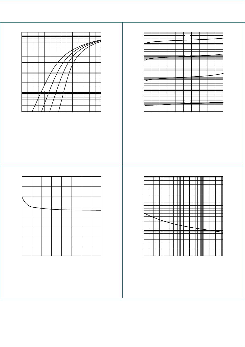
Fig 1. Forward current as a function of forward
voltage; typical values
Fig 2. Reverse current as a function of reverse
voltage; typical values
f=1MHz; T
amb
=25°C Based on square wave currents.
T
j
=25°C; prior to surge
Fig 3. Diode capacitance as a function of reverse
voltage; typical values
Fig 4. Non-repetitive peak forward current as a
function of pulse duration; maximum values
006aab132
1
10
10
2
10
3
I
F
(mA)
10
1
V
F
(V)
0 1.41.00.4 0.80.2 1.20.6
(1) (2) (3) (4)
006aab133
10
2
I
R
(μA)
V
R
(V)
0 1008040 6020
10
1
10
1
10
2
10
3
10
4
10
5
(1)
(2)
(3)
(4)
0816124
0.8
0.6
0
0.4
0.2
mbg446
V
R
(V)
C
d
(pF
)
mbg704
10
1
10
2
I
FSM
(A)
10
1
t
p
(μs)
110
4
10
3
10 10
2

BAV99,215

Mfr. #:
Manufacturer:
Nexperia
Description:
Diodes - General Purpose, Power, Switching SW DBL 100V 215MA HS
Lifecycle:
New from this manufacturer.
Delivery:
DHL FedEx Ups TNT EMS
Payment:
T/T Paypal Visa MoneyGram Western Union