2005-2013 Microchip Technology Inc. DS21946B-page 1
TC4421A/TC4422A
Features
• High Peak Output Current: 10A (typ.)
• Low Shoot-Through/Cross-Conduction Current in
Output Stage
• Wide Input Supply Voltage Operating Range:
- 4.5V to 18V
• High Continuous Output Current: 2A (max.)
• Matched Fast Rise and Fall Times:
- 15 ns with 4,700 pF Load
- 135 ns with 47,000 pF Load
• Matched Short Propagation Delays: 42 ns (typ.)
• Low Supply Current:
- With Logic ‘1’ Input – 130 µA (typ.)
- With Logic ‘0’ Input – 33 µA (typ.)
• Low Output Impedance: 1.2 (typ.)
• Latch-Up Protected: Will Withstand 1.5A Output
Reverse Current
• Input Will Withstand Negative Inputs Up To 5V
• Pin-Compatible with the TC4420/TC4429
and TC4421/TC4422 MOSFET Drivers
• Space-Saving, Thermally-Enhanced, 8-Pin DFN
Package
Applications
• Line Drivers for Extra Heavily-Loaded Lines
• Pulse Generators
• Driving the Largest MOSFETs and IGBTs
• Local Power ON/OFF Switch
• Motor and Solenoid Driver
• LF Initiator
General Description
The TC4421A/TC4422A are improved versions of the
earlier TC4421/TC4422 family of single-output
MOSFET drivers. These devices are high-current buf-
fer/drivers capable of driving large MOSFETs and Insu-
lated Gate Bipolar Transistors (IGBTs). The
TC4421A/TC4422A have matched output rise and fall
times, as well as matched leading and falling-edge
propagation delay times. The TC4421A/TC4422A
devices also have very low cross-conduction current,
reducing the overall power dissipation of the device.
These devices are essentially immune to any form of
upset, except direct overvoltage or over-dissipation.
They cannot be latched under any conditions within
their power and voltage ratings. These parts are not
subject to damage or improper operation when up to
5V of ground bounce is present on their ground
terminals. They can accept, without damage or logic
upset, more than 1A inductive current of either polarity
being forced back into their outputs. In addition, all
terminals are fully protected against up to 4 kV of
electrostatic discharge.
The TC4421A/TC4422A inputs may be driven directly
from either TTL or CMOS (3V to 18V). In addition,
300 mV of hysteresis is built into the input, providing
noise immunity and allowing the device to be driven
from slowly rising or falling waveforms.
With both surface-mount and pin-through-hole
packages, in addition to a wide operating temperature
range, the TC4421A/TC4422A family of 9A MOSFET
drivers fit into most any application where high gate/line
capacitance drive is required.
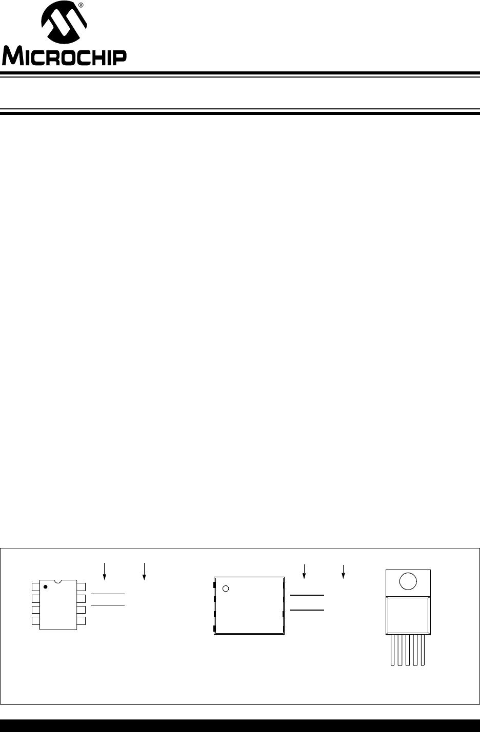
Package Types
(1)
8-Pin
1
2
3
4
V
DD
5
6
7
8
OUTPUT
GND
V
DD
INPUT
NC
GND
OUTPUT
TC4421A
TC4422A
5-Pin TO-220
V
DD
GND
INPUT
GND
OUTPUT
TC4421A
TC4422A
Tab is
Common
to V
DD
Note 1: Duplicate pins must both be connected for proper operation.
2: Exposed pad of the DFN package is electrically isolated.
TC4421A TC4422A
V
DD
OUTPUT
GND
OUTPUT
PDIP/SOIC
8-Pin DFN
(2)
V
DD
INPUT
NC
GND
2
3
4
5
6
7
8
1
TC4421A
TC4422A
V
DD
OUTPUT
GND
OUTPUT
TC4421A TC4422A
V
DD
OUTPUT
GND
OUTPUT
9A High-Speed MOSFET Drivers