© Semiconductor Components Industries, LLC, 2015
April, 2015 − Rev. 18
1 Publication Order Number:
NCS2200/D
NCS2200, NCS2200A,
NCV2200, NCS2202A
Low Voltage Comparators
The NCS2200 Series is an industry first sub−one volt, low power
comparator family. These devices consume only 10 mA of supply
current. They are guaranteed to operate at a low voltage of 0.85 V
which allows them to be used in systems that require less than 1.0 V
and are fully operational up to 6.0 V which makes them convenient for
use in both 3.0 V and 5.0 V systems. Additional features include no
output phase inversion with overdriven inputs, internal hysteresis,
which allows for clean output switching, and rail−to−rail input and
output performance. The NCS2200 Series is available in
complementary and open drain outputs and a variety of packages.
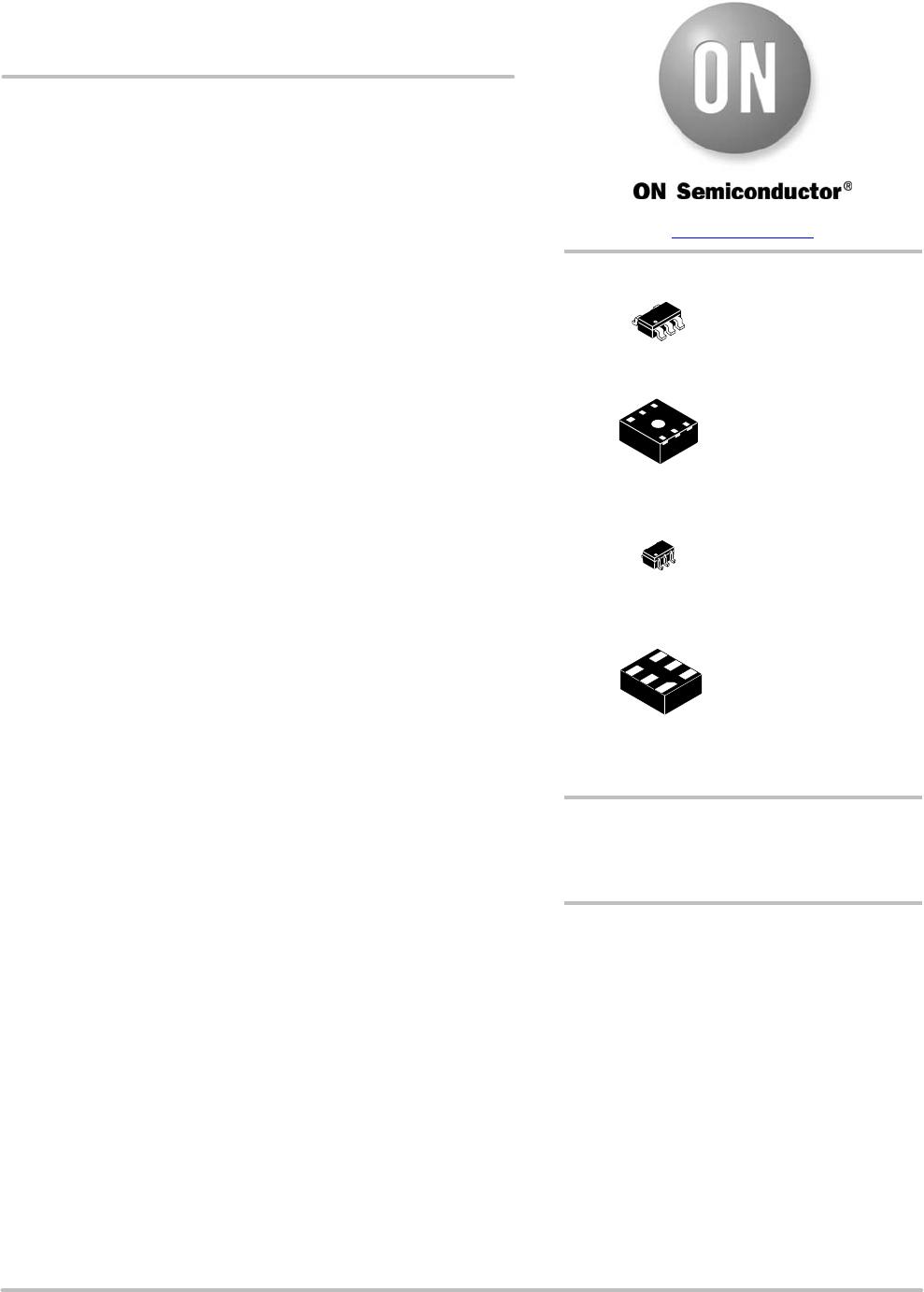
There are two industry standard pinouts for SOT−23−5 and
SC70−5 packages. The NCS2200 is also available in the tiny DFN
2x2.2 package. The NCS2200A and NCS2202A are available in
UDFN 1.2x1.0 package. See package option information in Table 1 on
page 2 for more information.
Features
Operating Voltage of 0.85 V to 6.0 V
Rail−to−Rail Input/Output Performance
Low Supply Current of 10 mA
No Phase Inversion with Overdriven Input Signals
Glitchless Transitioning in or out of Tri−State Mode
Complementary or Open Drain Output Configuration
Internal Hysteresis
Propagation Delay of 1.0 ms for NCS2200
NCV Prefix for Automotive and Other Applications Requiring
Unique Site and Control Change Requirements; AEC−Q100
Qualified and PPAP Capable
These Devices are Pb−Free and are RoHS Compliant
Typical Applications
Single Cell NiCd/NiMH Battery Powered Applications
Automotive
End Products
Cellphones, Smart Phones
Alarm and Security Systems
Personal Digital Assistants
DFN 2x2.2
SQL SUFFIX
CASE 488
SOT−23−5 (TSOP−5)
SN SUFFIX
CASE 483
See detailed ordering and shipping information in the package
dimensions section on page 13 of this data sheet.
ORDERING INFORMATION
See general marking information in the device marking
section on page 14 of this data sheet.
DEVICE MARKING INFORMATION
www.onsemi.com
SC70−5
SQ SUFFIX
CASE 419A
5
1
1
6
5
1
UDFN 1.2x1.0
MU SUFFIX
CASE 517AA
1
NCS2200, NCS2200A, NCV2200, NCS2202A
www.onsemi.com
2
Table 1. COMPARATOR SELECTOR GUIDE
Output Type Device Package Pinout Style
Complementary NCS2200AMUT1G UDFN, 1.2x1.0 N/A
Complementary NCS2200SN1T1G SOT−23−5 1
Complementary NCV2200SN1T1G* SOT−23−5 1
Complementary NCS2200SN2T1G SOT−23−5 2
Complementary NCV2200SN2T1G* SOT−23−5 2
Complementary NCS2200SQ2T2G SC70−5 2
Complementary NCV2200SQ2T2G* SC70−5 2
Complementary NCS2200SQLT1G DFN, 2x2.2 N/A
Open Drain NCS2202SN1T1G SOT−23−5 1
Open Drain NCS2202SN2T1G SOT−23−5 2
Open Drain NCV2202SN2T1G* SOT−23−5 2
Open Drain NCS2202SQ1T2G SC70−5 1
Open Drain NCS2202SQ2T2G SC70−5 2
Open Drain NCS2202AMUTBG UDFN, 1.2 x 1.0 N/A
*NCV Prefix for Automotive and Other Applications Requiring Unique Site and Control Change Requirements; AEC−Q100 Qualified and PPAP
Capable.
1
3
V
OUT
IN−
2
V
CC
V
EE
4
IN+
5
6
NC
PIN CONNECTIONS
1
Output
V
CC
Non−Inverting
Input
2
3
5
4
V
EE
Inverting
Input
1
Output
V
EE
Non−Inverting
Input
2
3
5
4
V
CC
Inverting
Input
Figure 1. SOT−23−5 (NCS2200, NCS2202), SC70−5 (NCS2200, NCS2202)
Style 1 Pinout (SN1T1)
Style 2 Pinout (SN2T1, SQ2T2)
-
+
-
+
Figure 2. DFN 2x2.2 (NCS2200)
Top View
1
3
V
OUT
IN−
2
NC
V
EE
4
IN+
5
6
V
CC
Figure 3. UDFN 1.2x1.0
(NCS2200A/NCS2202A)
Top View
NCS2200, NCS2200A, NCV2200, NCS2202A
www.onsemi.com
3
MAXIMUM RATINGS
Rating Symbol Value Unit
Supply Voltage Range (V
CC
to V
EE
) V
S
6.0 V
Non−inverting/Inverting Input to V
EE
V
CM
−0.2 to (V
CC
+ 0.2) V
Operating Junction Temperature T
J
150 °C
Operating Ambient Temperature Range
NCS2200, NCS2202, NCS2200A, NCS2202A
NCV2200, NCV2202
T
A
−40 to +105
−40 to +125
°C
Storage Temperature Range T
stg
−65 to +150 °C
Output Short Circuit Duration Time (Note 1) t
S
Indefinite s
ESD Tolerance (Note 2)
NCS2200
Human Body Model
Machine Model
NCS2202
Human Body Model
Machine Model
NCS2200A
Human Body Model
Machine Model
NCS2202A
Human Body Model − all pins except output
Human Body Model − output pin
Machine Model
ESD
HBM
MM
HBM
MM
HBM
MM
HBM
HBM
MM
2000
200
2000
200
1900
200
1500
500
150
V
Thermal Resistance, Junction−to−Ambient
TSOP−5
DFN (Note 3)
SC70−5
UDFN
R
q
JA
238
215
283
350
°C/W
Stresses exceeding those listed in the Maximum Ratings table may damage the device. If any of these limits are exceeded, device functionality
should not be assumed, damage may occur and reliability may be affected.
1. The maximum package power dissipation limit must not be exceeded.
P
D
+
T
J(max)
* T
A
R
qJA
2. ESD data available upon request.
3. For more information, refer to application note, AND8080/D.

NCV2200AMUTBG

Mfr. #:
Manufacturer:
ON Semiconductor
Description:
Analog Comparators ANA COMPARATOR UDFN6
Lifecycle:
New from this manufacturer.
Delivery:
DHL FedEx Ups TNT EMS
Payment:
T/T Paypal Visa MoneyGram Western Union