NCS2200, NCS2200A, NCV2200, NCS2202A
www.onsemi.com
13
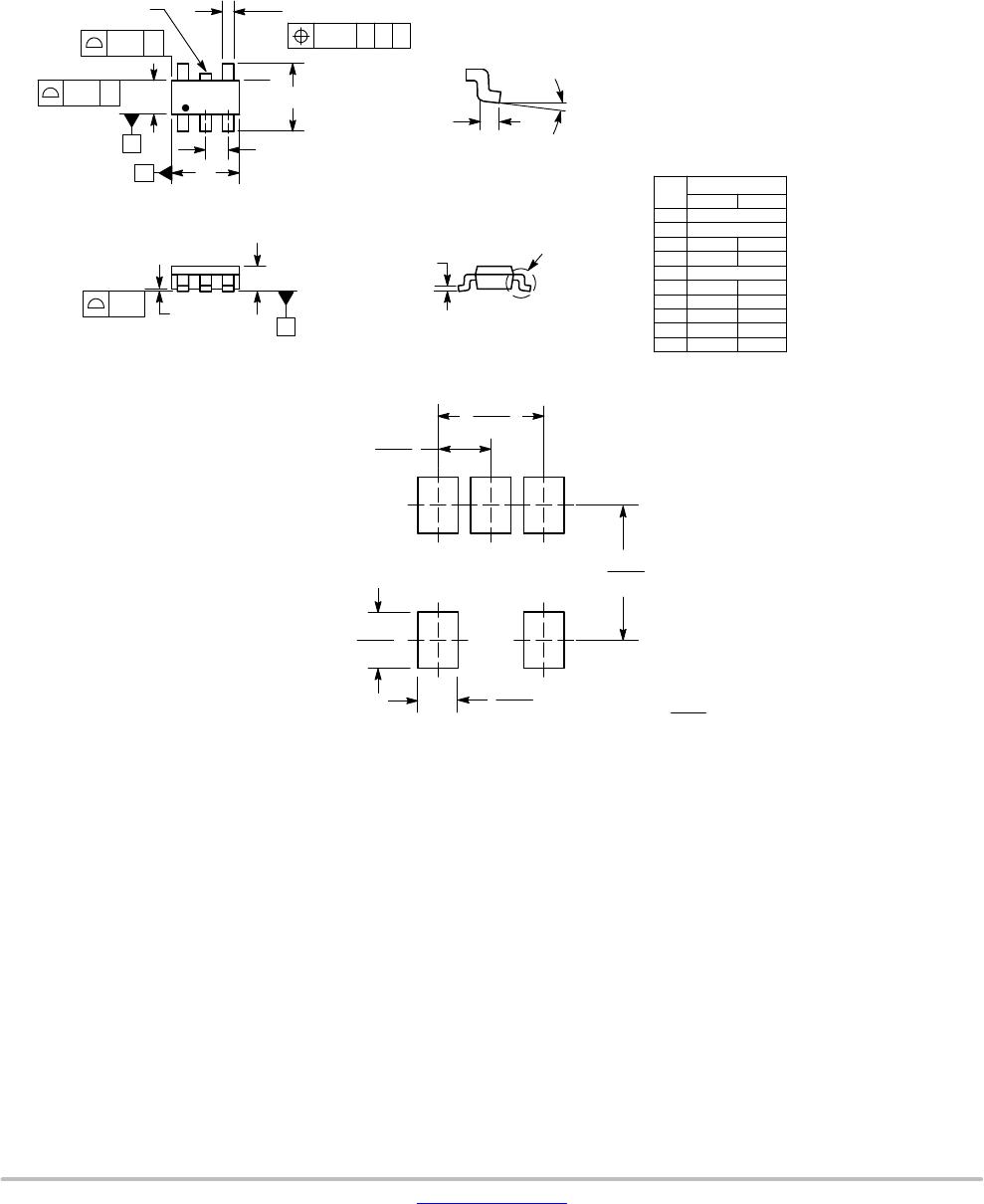
ORDERING INFORMATION
Device Pinout Style Output Type Package Shipping
NCS2200AMUT1G N/A Complementary UDFN
(Pb−Free)
3000 / Tape & Reel
NCS2200SN1T1G 1 Complementary SOT−23−5 (TSOP−5)
(Pb−Free)
3000 / Tape & Reel
NCV2200SN1T1G* 1 Complementary SOT−23−5 (TSOP−5)
(Pb−Free)
3000 / Tape & Reel
NCS2200SN2T1G 2 Complementary SOT−23−5 (TSOP−5)
(Pb−Free)
3000 / Tape & Reel
NCV2200SN2T1G* 2 Complementary SOT−23−5 (TSOP−5)
(Pb−Free)
3000 / Tape & Reel
NCS2200SQ2T2G 2 Complementary SC70−5
(Pb−Free)
3000 / Tape & Reel
NCV2200SQ2T2G* 2 Complementary SC70−5
(Pb−Free)
3000 / Tape & Reel
NCS2200SQLT1G N/A Complementary DFN, 2x2.2
(Pb−Free)
3000 / Tape & Reel
NCS2202SN1T1G 1 Open Drain SOT−23−5 (TSOP−5)
(Pb−Free)
3000 / Tape & Reel
NCS2202SN2T1G 2 Open Drain SOT−23−5 (TSOP−5)
(Pb−Free)
3000 / Tape & Reel
NCV2202SN2T1G* 2 Open Drain SOT−23−5 (TSOP−5)
(Pb−Free)
3000 / Tape & Reel
NCS2202SQ1T2G 1 Open Drain SC70−5
(Pb−Free)
3000 / Tape & Reel
NCS2202SQ2T2G 2 Open Drain SC70−5
(Pb−Free)
3000 / Tape & Reel
NCS2202AMUTBG N/A Open Drain UDFN
(Pb−Free)
3000 / Tape & Reel
This device contains 93 active transistors.
For information on tape and reel specifications, including part orientation and tape sizes, please refer to our Tape and Reel Packaging
Specifications Brochure, BRD8011/D.
*NCV Prefix for Automotive and Other Applications Requiring Unique Site and Control Change Requirements; AEC−Q100 Qualified and
PPAP Capable.
NCS2200, NCS2200A, NCV2200, NCS2202A
www.onsemi.com
14
x = I for NCS2200SN1T1
J for NCS2200SN2T1
M for NCS2202SN1T1
N for NCS2202SN2T1
A = Assembly Location
Y = Year
W = Work Week
G = Pb−Free Package
MARKING DIAGRAMS
SOT−23−5
(TSOP−5)
SN SUFFIX
CASE 483
CB = Specific Device Code
M = Date Code*
G = Pb−Free Package
DFN6 2x2.2
SQL SUFFIX
CASE 488
CBx MG
G
SC70−5
SQ SUFFIX
CASE 419A
CBx = Specific Device Code
x = A for NCS2200SQ2T2
D for NCS2202SQ1T2G
E for NCS2202SQ2T2G
M = Date Code*
G = Pb−Free Package
1
5
(Note: Microdot may be in either location)
1
5
CAx AYWG
G
(Note: Microdot may be in either location)
x S for Specific Device Code
V for NCS2202A (V with 180° Rotation)
M = Date Code
G = Pb−Free Package
x M
G
(Top View)
UDFN6 1.2x1.0
MU SUFFIX
CASE 517AA
CB MG
G
*Date Code overbar and underbar may vary
depending upon manufacturing location.
*Date Code orientation, position, and underbar
may vary depending upon manufacturing loc-
ation.
1
1
NCS2200, NCS2200A, NCV2200, NCS2202A
www.onsemi.com
15
PACKAGE DIMENSIONS
SOT−23−5 / TSOP−5 / SC59−5
SN SUFFIX
CASE 483−02
ISSUE K
NOTES:
1. DIMENSIONING AND TOLERANCING PER ASME
Y14.5M, 1994.
2. CONTROLLING DIMENSION: MILLIMETERS.
3. MAXIMUM LEAD THICKNESS INCLUDES LEAD FINISH
THICKNESS. MINIMUM LEAD THICKNESS IS THE
MINIMUM THICKNESS OF BASE MATERIAL.
4. DIMENSIONS A AND B DO NOT INCLUDE MOLD
FLASH, PROTRUSIONS, OR GATE BURRS. MOLD
FLASH, PROTRUSIONS, OR GATE BURRS SHALL NOT
EXCEED 0.15 PER SIDE. DIMENSION A.
5. OPTIONAL CONSTRUCTION: AN ADDITIONAL
TRIMMED LEAD IS ALLOWED IN THIS LOCATION.
TRIMMED LEAD NOT TO EXTEND MORE THAN 0.2
FROM BODY.
DIM MIN MAX
MILLIMETERS
A 3.00 BSC
B 1.50 BSC
C 0.90 1.10
D 0.25 0.50
G 0.95 BSC
H 0.01 0.10
J 0.10 0.26
K 0.20 0.60
M 0 10
S 2.50 3.00
123
54
S
A
G
B
D
H
C
J
__
0.7
0.028
1.0
0.039
ǒ
mm
inches
Ǔ
SCALE 10:1
0.95
0.037
2.4
0.094
1.9
0.074
*For additional information on our Pb−Free strategy and soldering
details, please download the ON Semiconductor Soldering and
Mounting Techniques Reference Manual, SOLDERRM/D.
SOLDERING FOOTPRINT*
0.20
5X
C AB
T0.10
2X
2X
T0.20
NOTE 5
C
SEATING
PLANE
0.05
K
M
DETAIL Z
DETAIL Z
TOP VIEW
SIDE VIEW
A
B
END VIEW

NCV2200AMUTBG

Mfr. #:
Manufacturer:
ON Semiconductor
Description:
Analog Comparators ANA COMPARATOR UDFN6
Lifecycle:
New from this manufacturer.
Delivery:
DHL FedEx Ups TNT EMS
Payment:
T/T Paypal Visa MoneyGram Western Union