8302 Data Sheet
©2016 Integrated Device Technology, Inc Revision D March 4, 20164
TABLE 4B. AC CHARACTERISTICS, V
DD
= 3.3V±5%, V
DDO
= 2.5V±5%, TA = 0°C TO 70°C
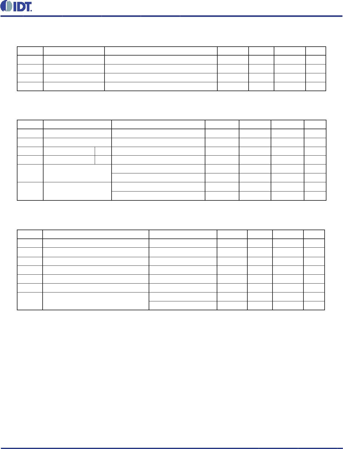
TABLE 3C. POWER SUPPLY DC CHARACTERISTICS, V
DD
= 3.3V±5%, V
DDO
= 2.5V±5%, TA = 0°C TO 70°C
Symbol Parameter Test Conditions Minimum Typical Maximum Units
V
DD
Core Supply Voltage 3.135 3.3 3.465 V
V
DDO
Output Supply Voltage 2.375 2.5 2.625 V
I
DD
Power Supply Current 13 mA
I
DDO
Output Supply Current 4mA
TABLE 3D. LVCMOS / LVTTL DC CHARACTERISTICS, V
DD
= 3.3V±5%, V
DDO
= 2.5V±5%, TA = 0°C TO 70°C
Symbol Parameter Test Conditions Minimum Typical Maximum Units
V
IH
Input High Voltage 2 V
DD
+ 0.3 V
V
IL
Input Low Voltage -0.3 0.8 V
I
IH
Input High Current CLK V
DD
= V
IN
= 3.465V 150 µA
I
IL
Input Low Current CLK V
DD
= 3.465V, V
IN
= 0V -5 µA
V
OH
Output High Voltage
50Ω to V
DDO
/2
1.8 V
I
OH
= -100µA 2.2 V
V
OL
Output Low Voltage
50Ω to V
DDO
/2
0.5 V
I
OL
= 100µA 0.2
V
Symbol Parameter Test Conditions Minimum Typical Maximum Units
f
MAX
Output Frequency 200 MHz
tp
LH
Propagation Delay, Low-to-High; NOTE 1
ƒ ≤ 200MHz
2.3 3.3 ns
tsk(o) Output Skew; NOTE 2, 4 85 ps
tsk(pp) Part-to-Part Skew; NOTE 3, 4 250 800 ps
t
R
Output Rise Time 20% to 80% 250 650 ps
t
F
Output Fall Time 20% to 80% 250 650 ps
odc Output Duty Cycle
ƒ ≤ 133MHz
45 55 %
133MHz < ƒ ≤ 200MHz
40
60 %
Parameters measured at f
MAX
unless otherwise noted.
NOTE 1: Measured from V
DD
/2 of the input to V
DDO
/2 of the output.
NOTE 2: Defi ned as skew between outputs at the same supply voltage and with equal load conditions.
Measured at V
DDO
/2.
NOTE 3: Defi ned as skew between outputs on different devices operating at the same supply voltages
and with equal load conditions. Using the same type of inputs on each device, the outputs are measured
at V
DDO
/2.
NOTE 4: This parameter is defi ned in accordance with JEDEC Standard 65.


