8
LT1961
1961fa
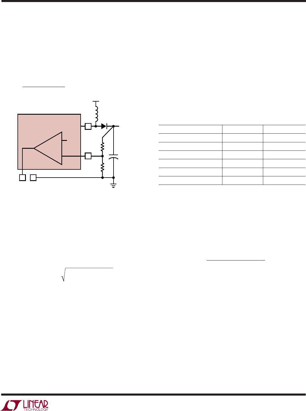
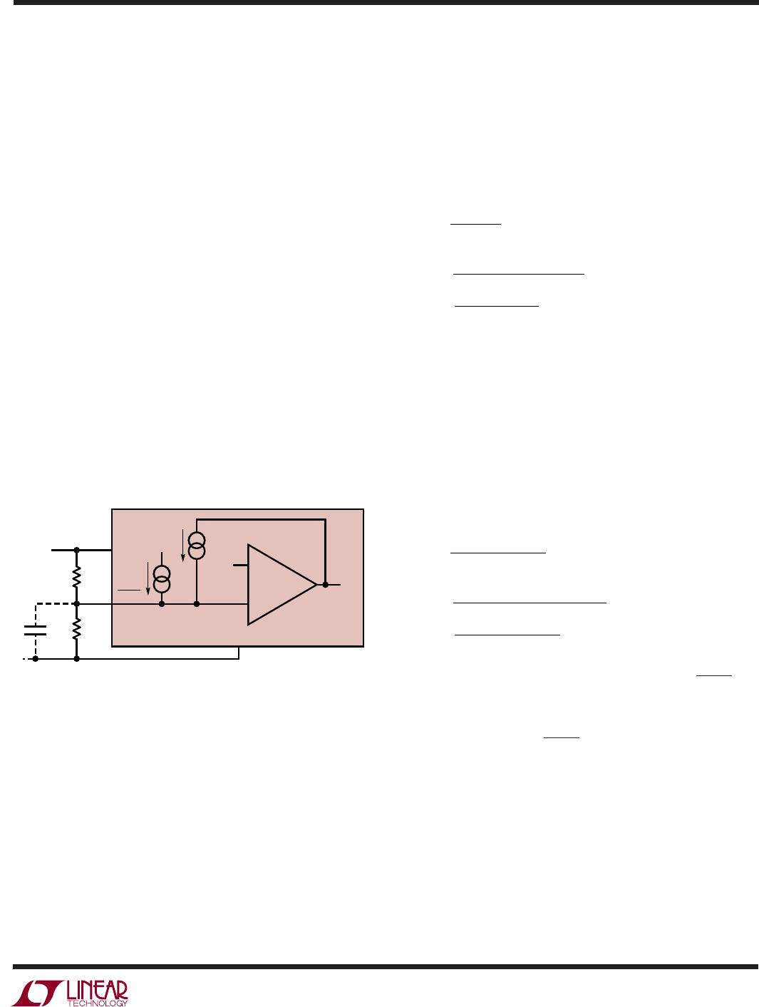
APPLICATIONS INFORMATION
WUU
U
INDUCTOR CHOICE AND MAXIMUM OUTPUT
CURRENT
When choosing an inductor, there are 2 conditions that
limit the minimum inductance; required output current,
and avoidance of subharmonic oscillation. The maximum
output current for the LT1961 in a standard boost con-
verter configuration with an infinitely large inductor is:
IA
V
V
OUT MAX
IN
OUT
()
.
•
= 15
η
Where η = converter efficiency (typically 0.87 at high
current).
As the value of inductance is reduced, ripple current
increases and I
OUT(MAX)
is reduced. The minimum induc-
tance for a required output current is given by:
L
VV V
Vf
VI
V
MIN
IN OUT IN
OUT
OUT OUT
IN
=
⎛
⎝
⎜
⎞
⎠
⎟
(–)
() . –
()()
•
215
η
The second condition, avoidance of subharmonic oscilla-
tion, must be met if the operating duty cycle is greater than
50%. The slope compensation circuit within the LT1961
prevents subharmonic oscillation for inductor ripple cur-
rents of up to 0.7A
P-P
, defining the minimum inductor
value to be:
L
VV V
Vf
MIN
IN OUT IN
OUT
=
(–)
.()07
These conditions define the absolute minimum induc-
tance. However, it is generally recommended that to
prevent excessive output noise, and difficulty in obtaining
stability, the ripple current is no more than 40% of the
average inductor current. Since inductor ripple is:
I
VV V
VLf
P P RIPPLE
IN OUT IN
OUT
−
=
(–)
()()
The recommended minimum inductance is:
L
VV V
VIf
MIN
IN OUT IN
OUT OUT
=
()( – )
. ( ) ( )( )
2
2
04
The inductor value may need further adjustment for other
factors such as output voltage ripple and filtering require-
ments. Remember also, inductance can drop significantly
with DC current and manufacturing tolerance.
The inductor must have a rating greater than its peak
operating current to prevent saturation resulting in effi-
ciency loss. Peak inductor current is given by:
I
VI
V
VV V
VLf
LPEAK
OUT OUT
IN
IN OUT IN
OUT
=+
−()()
•
()
()()η 2
Also, consideration should be given to the DC resistance
of the inductor. Inductor resistance contributes directly to
the efficiency losses in the overall converter.
Suitable inductors are available from Coilcraft, Coiltronics,
Dale, Sumida, Toko, Murata, Panasonic and other manu-
factures.
Table 2
PART NUMBER VALUE (uH) I
SAT(DC)
(Amps) DCR (Ω) HEIGHT (mm)
Coiltronics
TP1-2R2 2.2 1.3 0.188 1.8
TP2-2R2 2.2 1.5 0.111 2.2
TP3-4R7 4.7 1.5 0.181 2.2
TP4- 100 10 1.5 0.146 3.0
Murata
LQH1C1R0M04 1.0 0.51 0.28 1.8
LQH3C1R0M24 1.0 1.0 0.06 2.0
LQH3C2R2M24 2.2 0.79 0.1 2.0
LQH4C1R5M04 1.5 1 0.09 2.6
Sumida
CD73- 100 10 1.44 0.080 3.5
CDRH4D18-2R2 2.2 1.32 0.058 1.8
CDRH5D18-6R2 6.2 1.4 0.071 1.8
CDRH5D28-100 10 1.3 0.048 2.8
Coilcraft
1008PS-272M 2.7 1.3 0.14 2.7
LPO1704-222M 2.2 1.6 0.12 1.0
LPO1704-332M 3.3 1.3 0.16 1.0