UPG2251T6M-A

+25 dBm MATCHED POWER AMPLIFIER FOR Bluetooth
TM
Class 1
GaAs INTEGRATED CIRCUIT
µ
PG2251T6M
Document No. PG10783EJ01V0DS (1st edition)
Date Published October 2009 NS
DESCRIPTION
The
µ
PG2251T6M is a fully matched, +25 dBm GaAs MMIC power amplifier for Bluetooth Class 1.
This device realizes high efficiency, high gain and high output power.
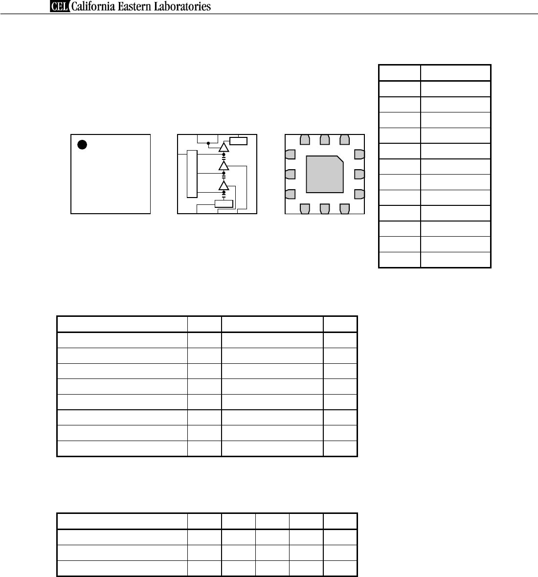
This device is housed in a 12-pin plastic TSQFN (T
hin Small Quad Flat Non-leaded) (T6M) package, and is
suitable for high-density surface mounting.
FEATURES
Operating frequency : fopt = 2 400 to 2 500 MHz (2 450 MHz TYP.)
• Supply voltage : V
DD1, 2, 3 = 2.5 to 3.5 V (3.0 V TYP.)
Control voltage : V
cont = 1.5 to 2.1 V (1.8 V TYP.)
• Circuit current : I
DD = 230 mA TYP. @ VDD1, 2, 3 = 3.0 V, Vcont = 1.8 V, Pout = +25 dBm
Output power : P
out = +25.0 dBm TYP. @ VDD1, 2, 3 = 3.0 V, Vcont = 1.8 V, Pin = 5 dBm
Gain control range : GCR = 70 dB TYP. @ V
DD1, 2, 3 = 3.0 V, Vcont = 0 to 1.8 V, Pin = 5 dBm
High efficiency : PAE = 47% TYP. @ V
DD1, 2, 3 = 3.0 V, Vcont = 1.8 V, Pin = 5 dBm
High-density surface mounting : 12-pin plastic TSQFN (T6M) package (2.0 × 2.0 × 0.37 mm)
APPLICATIONS
Power Amplifier for Bluetooth Class 1, ZigBee
TM
etc.
ORDERING INFORMATION
Part Number Order Number Package Marking Supplying Form
µ
PG2251T6M-E2
µ
PG2251T6M-E2-A 12-pin plastic TSQFN
(T6M) (Pb-Free)
2251 Embossed tape 8 mm wide
Pin 10, 11, 12 face the perforation side of the tape
Qty 3 kpcs/reel
Remark: To order evaluation samples, please contact your nearby sales office.
Part number for sample order:
µ
PG2251T6M-A
Caution: Observe precautions when handling, because these devices are sensitive to electrostatic discharge.
Data Sheet PG10783EJ01V0DS
2
µ
PG2251T6M
PIN CONNECTIONS AND INTERNAL BLOCK DIAGRAM
(Bottom View)
1
2
3
9
8
7
4
5
6
12
11
10
(Top View)
6
5
4
10
11
12
1
2
3
9
8
7
2251
(Top View)
6
5
4
10
11
12
1
2
3
9
8
7
Bias Circuit
M/N
M/N
Pin No. Pin Name
1 Vcont
2 GND
3 GND
4 Pin
5 VDD1
6 VDD2
7 GND
8 GND
9 GND
10 Pout
11 VDD3
12 VDD3
Remark Exposed pad : GND
ABSOLUTE MAXIMUM RATINGS (TA = +25°C, unless otherwise specified)
Parameter Symbol Ratings Unit
Supply Voltage VDD1, 2, 3 6.0 V
Control Voltage Vcont 3.0 V
Circuit Current IDD 300 mA
Control Current Icont 0.5 mA
Input Power Pin +10 dBm
Power Dissipation PD 600
Note
mW
Operating Ambient Temperature TA 40 to +85 °C
Storage Temperature Tstg 55 to +150 °C
Note Mounted on double-sided copper-clad 50 × 50 × 1.6 mm epoxy glass PWB, T
A = +85°C
RECOMMENDED OPERATING RANGE (TA = +25°C, unless otherwise specified)
Parameter Symbol MIN. TYP. MAX. Unit
Operating Frequency fopt 2 400 2 450 2 500 MHz
Supply Voltage VDD1, 2, 3 2.5 3.0 3.5 V
Control Voltage Vcont 1.5 1.8 2.1 V
Data Sheet PG10783EJ01V0DS
3
µ
PG2251T6M
ELECTRICAL CHARACTERISTICS (TA = +25°C, VDD1, 2, 3 = 3.0 V, Vcont = 1.8 V, f = 2.4 to 2.5 GHz,
unless otherwise specified)
Parameter Symbol Test Conditions MIN. TYP. MAX. Unit
Circuit Current IDD Pin = 5 dBm
230 265 mA
Output Power 1 Pout1 Pin = 5 dBm +23 +25
dBm
Output Power 2 Pout2 Vcont = 0 V, Pin = 5 dBm
45 30 dBm
Gain Control Range GCR Vcont = 0 to 1.8 V, Pin = 5 dBm
70
dB
Efficiency PAE Pin = 5 dBm
47
%
2nd Harmonics 2f0 Pin = 5 dBm
35
dBc
3rd Harmonics 3f0 Pin = 5 dBm
30
dBc
Input Return Loss RLin Pin = 30 dBm
5
dB
Output Return Loss RLout Pin = 30 dBm
10
dB
EVALUATION CIRCUIT
1
2
3
V
cont
P
out
P
in
4 5 6
9
8
7
12 11 10
390 pF
2.2 nH
0.1 F
µ
V
DD
1
0.1 F
µ
V
DD
2
6.8 nH
0.1 F
µ
V
DD
3
Bias Circuit
M/N
M/N
The application circuits and their parameters are for reference only and are not intended for use in actual design-ins.

UPG2251T6M-A

Mfr. #:
Manufacturer:
CEL
Description:
RF Amplifier 2.45GHz 3.0Volts -40C -85C
Lifecycle:
New from this manufacturer.
Delivery:
DHL FedEx Ups TNT EMS
Payment:
T/T Paypal Visa MoneyGram Western Union

Products related to this Datasheet