Expand menu
Hello, Sign in
My Account
0
Cart
Home
Products
Sensors
Semiconductors
Passive Components
Connectors
Power
Electromechanical
Optoelectronics
Circuit Protection
Integrated Circuits - ICs
Main Products
Manufacturers
Blog
Services
About OMO
About Us
Contact Us
Check Stock
UPG2251T6M-A
P1-P3
P4-P6
P7-P9
P10-P10
Data Sheet PG
10783EJ01V0DS
4
µ
PG2251T6M
TYPICAL CHARACT
ERISTICS
(T
A
= +25
°
C, V
DD
1, 2,
3 = 3.0 V, V
cont
= 1.8 V, f = 2.45
GHz, unless
otherw
ise s
pecified)
2f0
3f0
–20
–25
–30
–35
–40
–45
–50
–55
2
ND
HARMONICS, 3
RD
HARMONICS
vs.
INPUT PO
WER
2nd Harmonics 2f0 (dBc), 3rd Har
monics 3f0 (dBc)
Input P
ow
er P
in
(dBm)
–30
–20
–15
–10
0
–5
–25
5
P
out
I
DD
–30
–20
–15
–10
0
–5
–25
45
40
35
30
25
20
15
10
5
0
320
280
240
200
160
120
80
40
0
–
40
Gain
PA
E
OUTPUT PO
WER, GAIN, CIRCUIT
CURRENT
, P
AE vs
.
INPUT POWER
Input P
ow
er P
in
(dBm)
Circuit Current I
DD
(mA), Efficiency P
AE (%)
Output P
ow
er P
out
(dBm), Gain (dB)
Remark
The
graphs indicate no
minal characteristic
s.
Data Sheet PG
10783EJ01V0DS
5
µ
PG2251T6M
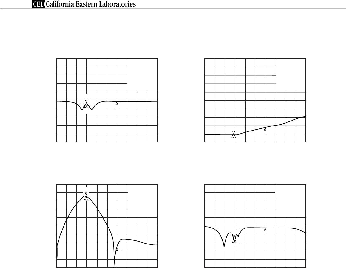
S-PARAMETE
RS
Condition : T
A
= +25
°
C, V
DD
1, 2,
3 =3
.0 V, V
cont
= 1.
8 V, P
in
=
−
30 dBm
S
22
-FREQUENCY
START 0.1 GHz STOP 8.1 GHz
1:
–15.2 dB
2:
–17.0 dB
3:
–15.0 dB
4:
–2.0 dB
0 dB
2
4
1
3
START 0.1 GHz STOP 8.1 GHz
0 dB
1:
35.9 dB
2:
35.5 dB
3:
34.8 dB
4:
–22.2 dB
S
21
-FREQUENCY
4
2
1
3
START 0.1 GHz STOP 8.1 GHz
0 dB
1:
–56.8 dB
2:
–53.6 dB
3:
–51.9 dB
4:
–42.5 dB
S
12
-FREQUENCY
2
1
3
4
START 0.1 GHz STOP 8.1 GHz
0 dB
1:
–4.3 dB
2:
–4.4 dB
3:
–4.8 dB
4:
–1.2 dB
1
3
4
S
11
-FREQUENCY
2
Remarks 1.
The graphs indic
ate nominal chara
cteristics.
2.
Maker 1 : 2.4 G
Hz, 2 : 2.
45 GHz, 3 :
2.5 GHz,
4 : 4.9 GHz
Data Sheet PG
10783EJ01V0DS
6
µ
PG2251T6M
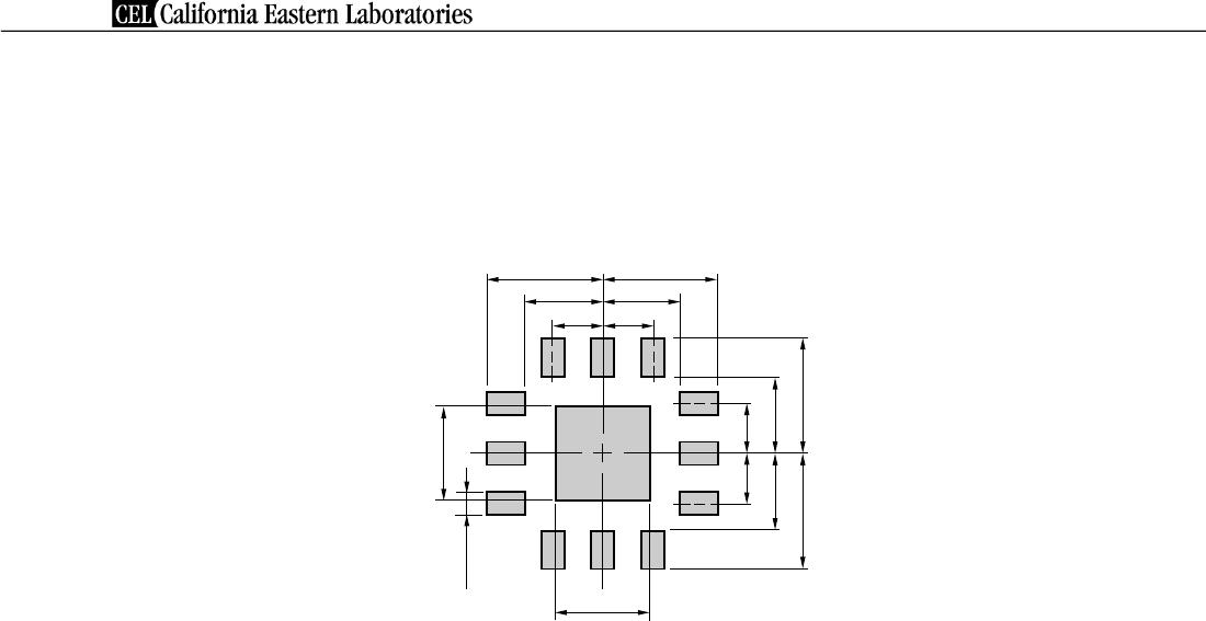
MOUNTING PA
D LAYOUT
DIMENSIONS
12-PIN PLASTI
C TSQFN (T6M) (UNIT: mm
)
MOUNTING P
AD
0.94
0.5
1.15
0.5
1.15
0.5
1.15
0.5
1.15
0.94
12–0.23
0.77
0.77
0.77
0.77
Remark
The mo
unting pad layout in this document is for reference only.
When designing PCB,
please consider workability of mounting,
solder joint reliability, prev
ention of solder
bridge and so on, in o
rder to optimize th
e design.
P1-P3
P4-P6
P7-P9
P10-P10
UPG2251T6M-A
Mfr. #:
Buy UPG2251T6M-A
Manufacturer:
CEL
Description:
RF Amplifier 2.45GHz 3.0Volts -40C -85C
Lifecycle:
New from this manufacturer.
Delivery:
DHL
FedEx
Ups
TNT
EMS
Payment:
T/T
Paypal
Visa
MoneyGram
Western
Union
Products related to this Datasheet
UPG2251T6M-A
UPG2251T6M-E2-A