Expand menu
Hello, Sign in
My Account
0
Cart
Home
Products
Sensors
Semiconductors
Passive Components
Connectors
Power
Electromechanical
Optoelectronics
Circuit Protection
Integrated Circuits - ICs
Main Products
Manufacturers
Blog
Services
About OMO
About Us
Contact Us
Check Stock
STW65N65DM2AG
P1-P3
P4-P6
P7-P9
P10-P12
STW
65N65DM2
AG
Electrica
l charact
eristics
DocID02
8164
Re
v
1
7/
12
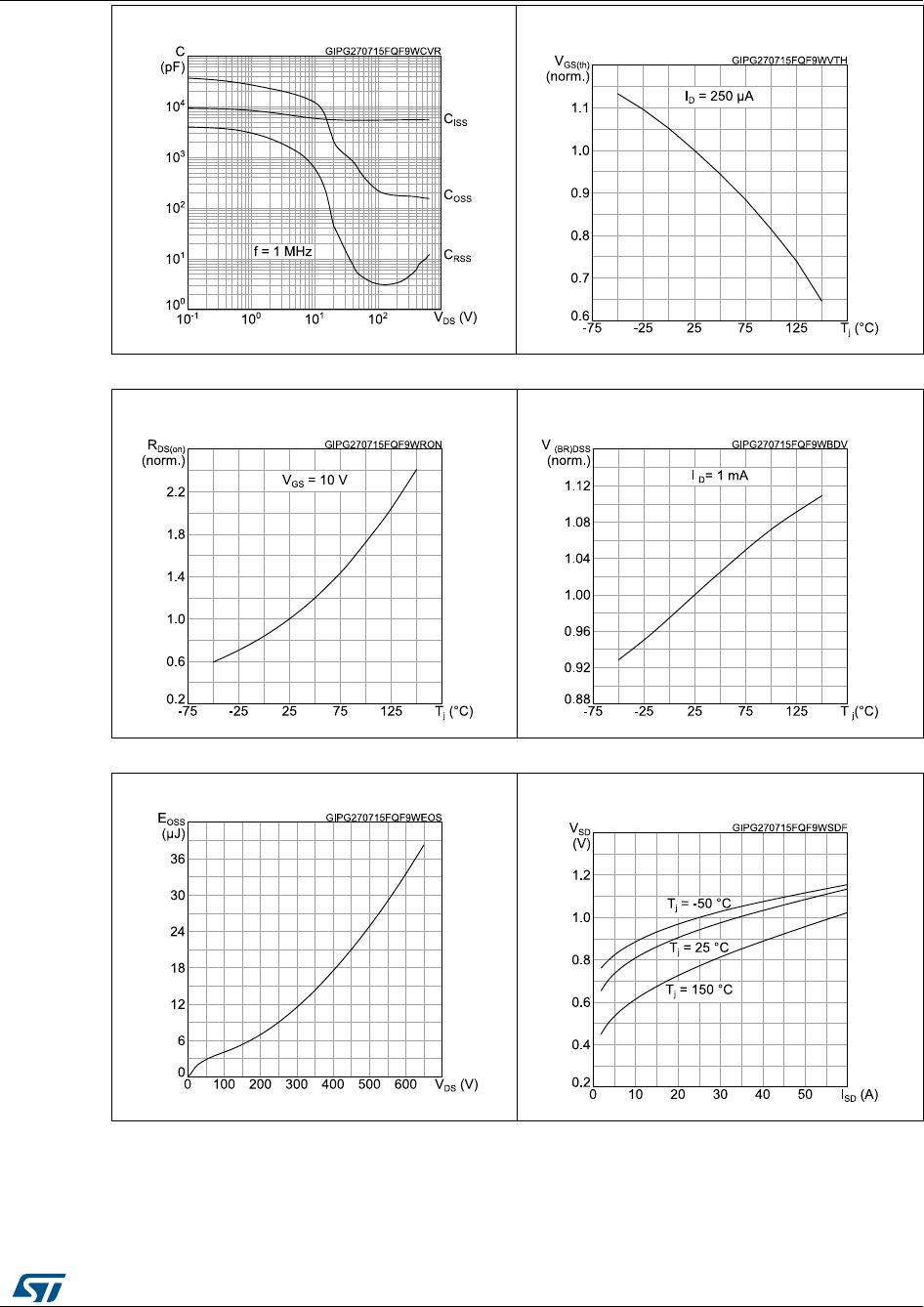
Figure
8
: Capaci
tanc
e variati
ons
Figure
9
: Nor
malized g
ate th
reshold vo
ltage
vs temperat
ure
Figure
10
: Normalized
on
-
re
sistance v
s
temperature
Figure
11
: Normaliz
ed V(BR)DSS vs
temperature
Figure
12
: Outpu
t capacitan
ce store
d energy
Figure
13
: Source
-
drain dio
de forward
characteri
stics
Test circu
its
STW
65N65D
M
2
AG
8/
12
DocID02
8164
Re
v
1
3
Test circuits
Figure
14
: Switchin
g times t
est circu
it for
resisti
ve
load
Figure
15
: Gate char
ge test
circuit
Figure
16
: Test circu
it for in
ductive load s
witching
and diode r
ecov
ery times
Figure
17
: Unclamped
indu
ctiv
e load test
circuit
Figure
18
: Unclamped
indu
ctiv
e waveform
Figure
19
: Switching time w
aveform
STW
65N65DM2
AG
Package
informati
on
DocID02
8164
Re
v
1
9/
12
4
Package inform
ation
In order t
o meet en
vironm
ental requ
irem
ents, ST of
fers thes
e devices
in diff
erent gr
ades of
ECOP
ACK
®
pack
ages, dep
ending on t
heir leve
l of env
ironm
ental com
pliance.
ECOPAC
K
®
specif
ications, grad
e def
initions and
product s
tatus are
availab
le at:
www.st.com
.
ECOP
ACK
®
is an ST
tradem
ark.
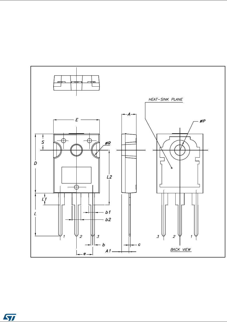
4.1
TO
-
247 package information
Figure
20
: TO
-
247 package
outli
ne
0075325_H
P1-P3
P4-P6
P7-P9
P10-P12
STW65N65DM2AG
Mfr. #:
Buy STW65N65DM2AG
Manufacturer:
STMicroelectronics
Description:
MOSFET Automotive-grade N-channel 650 V, 0.042 Ohm typ., 60 A MDmesh DM2 Power MOSFET in a TO-247 package
Lifecycle:
New from this manufacturer.
Delivery:
DHL
FedEx
Ups
TNT
EMS
Payment:
T/T
Paypal
Visa
MoneyGram
Western
Union
Products related to this Datasheet
STW65N65DM2AG