Typical Performance–AD1866
REV. 0
–3–
–100
–90
–80
–70
–60
–50
–40
–30
205005500500 15500
10500
FREQUENCY – Hz
THD+N – dB
–60dB
–20dB
0dB
Figure 1. THD+N vs. Frequency
125
120
123
121
10
3
122
10
2
124
10
4
FREQUENCY – Hz
CHANNEL SEPARATION – dB
10
5
Figure 2. Channel Separation vs. Frequency
–20dB
SUPPLY VOLTAGE
THD+N – dB
0dB
–30
–100
5.6
–70
–90
4.6
–80
4.4
–40
–60
–50
5.45.25.04.8
–60dB
Figure 3. THD+N vs. Supply Voltage
INPUT AMPLITUDE – dB
GAIN LINEARITY ERROR – dB
6
–8
20
–2
–6
–80
–4
–100
4
0
2
0
–20–40–60
125°C
–35°C
0°C
25°C
70°C
Figure 4. Gain Linearity Error vs. Input Amplitude
TEMPERATURE – °C
THD+N – dB
–30
–100
125
–70
–90
–50
–80
–75
–40
–60
–50
100755025
0
–25
–60dB
–20dB
0dB
Figure 5. THD+N vs. Temperature
FREQUENCY – Hz
PSRR – dB
80
40
10
3
10
5
70
50
10
4
60
Figure 6. Power Supply Rejection Ratio vs. Frequency
(Supply Modulation Amplitude at 500 mV p-p)
AD1866
REV. 0
–4–
ABSOLUTE MAXIMUM RATINGS*
V
L
to DGND . . . . . . . . . . . . . . . . . . . . . . . . . . . . . .0 V to 6 V
V
S
to AGND . . . . . . . . . . . . . . . . . . . . . . . . . . . . . .0 V to 6 V
AGND to DGND . . . . . . . . . . . . . . . . . . . . . . . . . . . . ±0.3 V
Digital Inputs to DGND . . . . . . . . . . . . . . . . . . . –0.3 V to V
L
Soldering (10 sec) . . . . . . . . . . . . . . . . . . . . . . . . . . . +300°C
*Stresses greater than those listed under “Absolute Maximum Ratings” may cause
permanent damage to the device. This is a stress rating only and functional
operation of the device at these or any other conditions above those indicated in the
operational section of this specification is not implied. Exposure to absolute
maximum rating conditions for extended periods may affect device reliability.
WARNING!
ESD SENSITIVE DEVICE
CAUTION
ESD (electrostatic discharge) sensitive device. Electrostatic charges as high as 4000 V readily
accumulate on the human body and test equipment and can discharge without detection.
Although the AD1866 features proprietary ESD protection circuitry, permanent damage may
occur on devices subjected to high energy electrostatic discharges. Therefore, proper ESD
precautions are recommended to avoid performance degradation or loss of functionality.
PIN CONFIGURATION
LL
DL
CLK
DR
LR
DGND
V
L
NRL
AGND
NRR
V
S
1
2
3
4
5
6
7
8
9
10
12
13
14
15
11
16
AD1866
16-BIT
DAC
16-BIT
DAC
16-BIT
SERIAL
REGISTER
16-BIT
SERIAL
REGISTER
V
B
L
V
O
R
V
S
V
B
R
V
REF
V
REF
V
O
L
PIN DESIGNATIONS
Pin Mnemonic Description
11V
L
Digital Supply (+5 V)
12 LL Left Channel Latch Enable Pin
13 DL Left Channel Data Input Pin
14 CLK Clock Input Pin
15 DR Right Channel Data Input Pin
16 LR Right Channel Latch Enable Pin
17 DGND Digital Common Pin
18V
B
R Right Channel Bias Pin
19V
S
Analog Supply (+5 V)
10 V
O
R Right Channel Output Pin
11 NRR Right Channel Noise Reduction Pin
12 AGND Analog Common Pin
13 NRL Left Channel Noise Reduction Pin
14 V
O
L Left Channel Output Pin
15 V
S
Analog Supply (+5 V)
16 V
B
L Left Channel Bias Pin
ORDERING GUIDE
Temperature Package Package
Model Range Description Option
AD1866N –35°C to +85°C Plastic DIP N-16
AD1866R –35°C to +85°C SOIC R-16
AD1866R-REEL –35°C to +85°C SOIC R-16
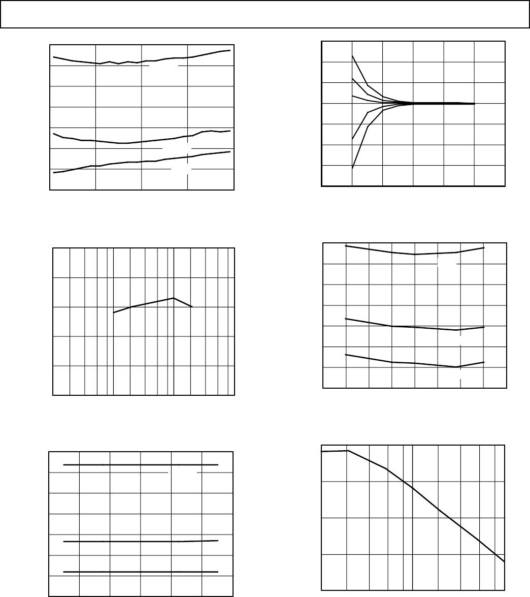
TOTAL HARMONIC DISTORTION + NOISE
Total harmonic distortion plus noise (THD+N) is defined as
the ratio of the square root of the sum of the squares of the am-
plitudes of the harmonics and noise to the amplitude of the fun-
damental input frequency. It is usually expressed in percent (%)
or decibels (dB).
D-RANGE DISTORTION (EIAJ SPECIFICATION)
D-Range distortion is the ratio of the amplitude of the signal at
an amplitude of –60 dB to the amplitude of the distortion plus
noise. In this case, an A-weight filter is used. The value speci-
fied for D-range performance is the ratio measured plus 60 dB.
SIGNAL-TO-NOISE RATIO
The signal-to-noise ratio is defined as the ratio of the amplitude
of the output when a full-scale output is present to the ampli-
tude of the output with no signal present. It is expressed in
decibels (dB) and measured using an A-weight filter.
GAIN LINEARITY
Gain linearity is a measure of the deviation of the actual output
amplitude from the ideal output amplitude. It is determined by
measuring the amplitude of the output signal as the amplitude
of that output signal is digitally reduced to a lower level. A per-
fect D/A converter exhibits no difference between the ideal and
actual amplitudes. Gain linearity is expressed in decibels (dB).
MIDSCALE ERROR
Midscale error, or bipolar zero error, is the deviation of the ac-
tual analog output from a voltage at the bias pin when the twos
complement input code representing midscale is loaded in the
DAC. Midscale error is expressed in mV.
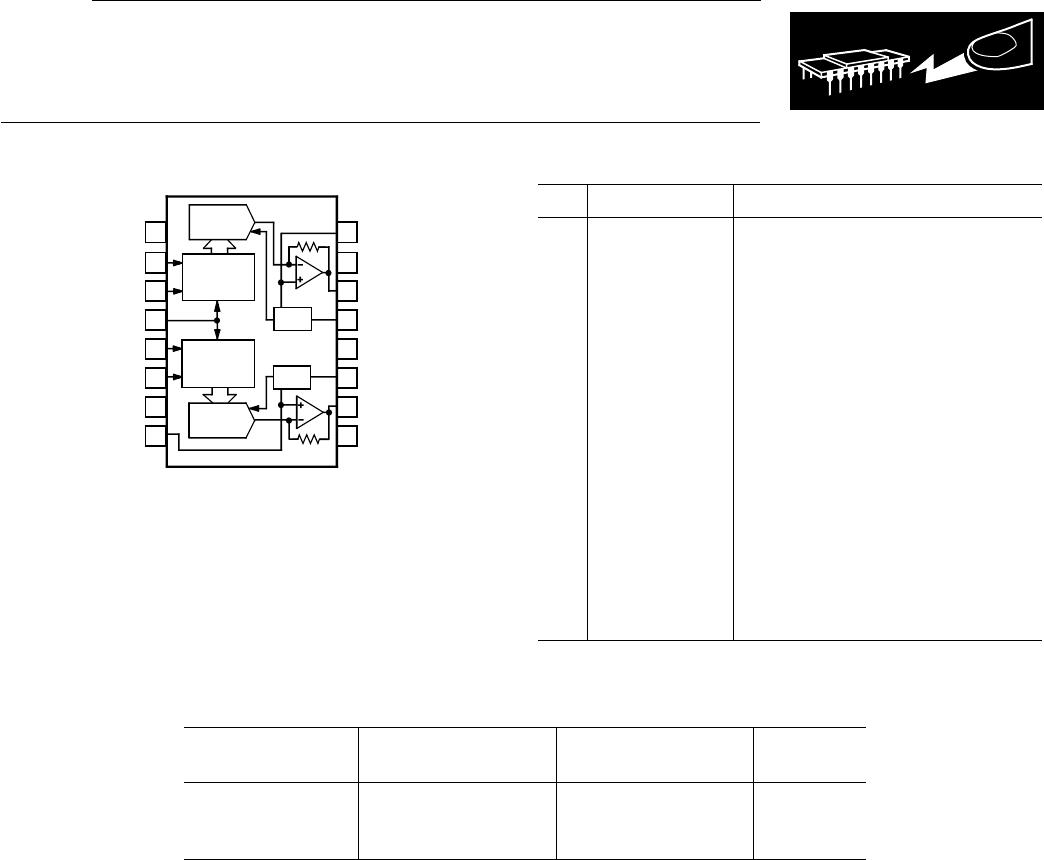
FUNCTIONAL DESCRIPTION
The AD1866 is a complete, monolithic dual 16-bit digital audio
DAC which runs off a single +5 volt supply. As shown in the
block diagram, each channel contains a voltage reference, a
16-bit serial-to-parallel input register, a 16-bit input latch, a
16-bit DAC, and an output amplifier.
The voltage reference section provides a reference voltage and a
false ground voltage for each channel. The low noise bandgap
circuits produce reference voltages that are unaffected by
changes in temperature, time, and power supply.
The input registers are fabricated with CMOS logic gates.
These gates allow high switching speeds and low power con-
sumption, contributing to the fast digital timing, the low glitch
and low power dissipation of the AD1866.
LL
DL
CLK
DR
LR
DGND
V
L
NRL
AGND
NRR
V
S
1
2
3
4
5
6
7
8
9
10
12
13
14
15
11
16
AD1866
16-BIT
DAC
16-BIT
DAC
16-BIT
SERIAL
REGISTER
16-BIT
SERIAL
REGISTER
V
B
L
V
O
R
V
S
V
B
R
V
REF
V
REF
V
O
L
AD1866 Functional Block Diagram
The 16-bit DAC uses a combination of segmentation and R-2R
architecture to achieve good integral and differential linearity.
The resistors which form the ladder structure are fabricated
with silicon-chromium thin film. Laser trimming of these resis-
tors further reduces linearity error, resulting in low output
distortion.
The output amplifier uses both MOS and bipolar devices and
incorporates an NPN class A output stage. It is designed to pro-
duce high slew rate, low noise, low distortion, and optimal fre-
quency response.
REV. 0
–5–
Definition of Specifications–AD1866

AD1866RZ-REEL

Mfr. #:
Manufacturer:
Analog Devices Inc.
Description:
Audio D/A Converter ICs IC +5V 116-Bit Audio
Lifecycle:
New from this manufacturer.
Delivery:
DHL FedEx Ups TNT EMS
Payment:
T/T Paypal Visa MoneyGram Western Union

Products related to this Datasheet