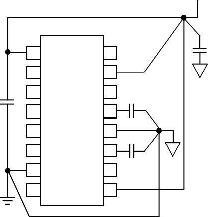
GROUNDING RECOMMENDATIONS
The AD1866 has two ground pins, designated as AGND (Pin
12) and DGND (Pin 7). The analog ground, AGND, serves as
the “high quality” reference ground for analog signals and as a
return path for the supply current from the analog portion of
the device. The system analog common should be located as
close as possible to Pin 12 to minimize any voltage drop which
may develop between these two points, although the internal
circuit is designed to minimize signal dependence of the analog
return current.
The digital ground, DGND, returns ground current from the
digital logic portion of the device. This pin should be connected
to the digital common node in the system. As shown in Figure
7, the analog and digital grounds should be joined at one point
in a system. When these two grounds are connected such as at
the power supply ground, care should be taken to minimize the
voltage difference between the DGND and AGND pins in or-
der to ensure the specified performance.
POWER SUPPLIES AND DECOUPLING
The AD1866 has three power supply input pins. V
S
(Pins 9 and
15) provide the supply voltages which operate the analog por-
tion of the device including the 16-bit DACs, the voltage refer-
ences, and the output amplifiers. The V
S
supplies are designed
to operate from a +5 V supply. These pins should be decoupled
to the analog ground using a 0.1 µF capacitor. Good engineer-
ing practice suggests that the bypass capacitor be placed as
close as possible to the package pins. This minimizes the inher-
ent inductive effects of printed circuit board traces.
V
L
(Pin 1) operates the digital portions of the chip including the
input shift registers and the input latching circuitry. V
L
is also
designed to operate from a +5 V supply. This pin should be by-
passed to digital common using a 0.1 µF capacitor, again placed
as close as possible to the package pins. Figure 7 illustrates the
correct connection of the digital and analog supply bypass
capacitors.
An important feature of the AD1866 audio DAC is its ability to
operate at diminished power supply voltages. This feature is
very important in portable battery operated systems. As the bat-
teries discharge, the supply voltage drops. Unlike any other au-
dio DAC, the AD1866 can continue to function at supply
voltages as low as 3.5 V. Because of its unique design, the
power requirements of the AD1866 diminish as the battery volt-
age drops, further extending the operating time of the system.
POWER
SUPPLY
4.7µF
4.7µF
(CAPACITOR VALUES ARE 0.1 µF UNLESS OTHERWISE
INDICATED)
15
14
13
12
11
10
16
9
1
2
3
4
5
6
8
7
NRL
AGND
NRR
AD1866
LL
DL
CLK
DR
LR
DGND
V
B
R
V
B
L
+
+
V
S
V
O
L
V
L
V
O
R
V
S
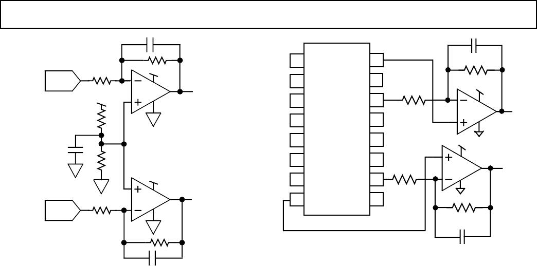
Figure 7. Recommended Circuit Schematic
NOISE REDUCTION CAPACITORS
The AD1866 has two noise reduction pins, designated as NRL
(Pin 13) and NRR (Pin 11). In order to meet specifications, it
is required that external noise reduction capacitors be con-
nected from these pins to AGND to reduce the output noise
contributed by the voltage reference circuitry. As shown in Fig-
ure 7, each of these pins should be bypassed to AGND with a
4.7 µF or larger capacitor. The connections between the ca-
pacitors, package pins and AGND should be as short as pos-
sible to achieve the lowest noise.
USING V
B
L AND V
B
R
The AD1866 has two bias voltage reference pins, designated as
V
B
R (Pin 8) and V
B
L (Pin 16). Each of these pins supplies a dc
reference voltage equal to the center of the output voltage swing.
These bias voltages replace “false ground” networks previously
required in single supply audio systems. At the same time, they
allow dc coupled systems, improving audio performance.
AD1866–Analog Circuit Considerations
REV. 0–6–
+
5V
+
5V
+
5V
FALSE GROUND
(2.5V)
V
O
R
V
O
L
V
O
R
V
O
L
Figure 8a. Schematic Using False Ground
Figure 8a illustrates the traditional approach used to generate
false ground voltages in single supply audio systems. This cir-
cuit requires additional power and circuit board space.
The AD1866 eliminates the need for “false ground” circuitry.
V
B
R and V
B
L generate the required bias voltages previously
generated by the “false ground.” As shown in Figure 8b, V
B
R
and V
B
L may be used as the reference point in each output
channel. This permits a dc coupled output signal path. This
eliminates ac coupling capacitors and improves low frequency
performance. It should be noted that these bias outputs have
relatively high output impedance and will not drive output cur-
rents larger than 100 µA without degrading the specified
performance.
Analog Circuit Considerations–AD1866
REV. 0
–7–
+5V
+5V
15
14
13
12
11
10
16
9
1
2
3
4
5
6
8
7
NRL
AGND
NRR
AD1866
LL
DL
CLK
DR
LR
DGND
V
O
L
V
O
R
V
O
R
V
S
V
B
R
V
O
L
V
S
V
L
V
B
L
Figure 8b. Circuitry Using Voltage Biases
DISTORTION PERFORMANCE AND TESTING
The THD+N figure of an audio DAC represents the amount of
undesirable signal produced during reconstruction and play-
back of an audio waveform. Therefore, the THD+N specifica-
tion provides a direct measure to classify and choose an audio
DAC for a desired level of performance. Figure 1 illustrates the
typical THD+N versus frequency performance of the AD1866.
It is evident that the THD+N performance of the AD1866 re-
mains stable at all three amplitude levels through a wide range
of frequencies. A load impedance of at least 2 k is recom-
mended for best THD+N performance.
Analog Devices tests all AD1866s on the basis of THD+N per-
formance. During the distortion test, a high speed digital pat-
tern generator transmits digital data to each channel of the
device under test. Sixteen-bit data is latched into the DAC at
352.8 kHz (8 × F
S
). The test input code is a digitally encoded
990.5 Hz sine wave with 0 dB, –20 dB, and –60 dB amplitudes.
A 4096 point FFT calculates total harmonic distortion + noise,
signal-to-noise ratio, and D-range. No deglitchers or external
adjustments are used.
AD1866–Digital Circuit Considerations
REV. 0–8–
L
S
B
M
S
B
M
S
B
L
S
B
CLK
DL
DR
LL
LR
Figure 9. AD1866 Control Signals
INPUT DATA
The digital input port of the AD1866 employs five signals: Data
Left (DL), Data Right (DR), Latch Left (LL), Latch Right
(LR), and Clock (CLK). DL and DR are the serial inputs for
the left and right DACs, respectively. Input data bits are clocked
into the input register on the rising edge of CLK. The falling
edges of LL and LR cause the last 16 bits which were clocked
into the serial registers to be shifted into the DACs, thereby up-
dating the respective DAC outputs. For systems using only a
single latch signal, LL and LR may be connected together. For
systems using only one DATA signal, DR and DL may be con-
nected together. Data is transmitted to the AD1866 in a bit
stream composed of 16-bit words with a serial, twos comple-
ment, MSB first format. Left and right channels share the Clock
(CLK) signal.
Figure 9 illustrates the general signal requirements for data
transfer for the AD1866.
TIMING
Figure 10 illustrates the specific timing requirements that must
be met in order for the data transfer to be accomplished prop-
erly. The input pins of the AD1866 are both TTL and +5 V
CMOS compatible.
>30ns
>10ns
>10ns
>30ns
>30ns
>15ns
>40ns
>40ns
DR/DL
CLK
LR/LL
>67ns
>40ns
Figure 10. AD1866 Input Signal Timing
The maximum clock rate of the AD1866 is specified to be at
least 13.5 MHz. This clock rate allows data transfer rates of 2×,
4×, 8×, and 16× F
S
(where F
S
equals 44.1 kHz). The applica-
tions section of this data sheet contains additional guidelines for
using the AD1866.

AD1866RZ-REEL

Mfr. #:
Manufacturer:
Analog Devices Inc.
Description:
Audio D/A Converter ICs IC +5V 116-Bit Audio
Lifecycle:
New from this manufacturer.
Delivery:
DHL FedEx Ups TNT EMS
Payment:
T/T Paypal Visa MoneyGram Western Union

Products related to this Datasheet