9
Using the ISL6119EVAL1 Platform
General and Biasing Information
The ISL6119EVAL1 platform, Figure 19, allows evaluation of
the ISL6119 dual power supply control IC and comparison
against a suitably sized PPTC component.
The evaluation platform is biased and monitored through
numerous test points (TP#). See Table 1 for test point
assignments and descriptions.
Upon proper bias the PPTC, F1 has a nominal 500mA load
current passing through it which is the hold current rating for
that particular device. Removal of the PPTC is necessary to
isolate the ISL6119 as the PPTC load current is common to
the ISL6119EVAL1 bias connections.
By enabling either or both of the ISL6119L switches by
signaling TP3 and/or TP4 low (<0.6V) these switches are
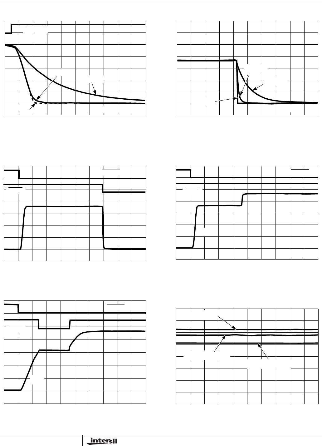
also loaded with a nominal 500mA current. See Figures 3
and 8 for typical ISL6119 turn-on and off waveforms.
Provided test points enable the evaluation of voltage loss
across the PPTC (TP9 - TP10) and the ISL6119 enabled
switches (TP9 - TP6 and TP7). Expect to see 50% - 300%
greater voltage loss across typical PPTC devices than the
ISL6119. See Figure 13 for a voltage loss comparison
across ISL6119 and PPTC device.
An overcurrent (OC) condition can be invoked on both the
ISL6119 and the PPTC by driving TP11 to +6V, causing SW1
to close and a nominal 1.5A load is imposed. This
represents a current over load to the ISL6119 and is thus
quickly current regulated to the 1A limit. If the OC duration
extends beyond the nominal 12ms of the internal ISL6119L
timer then the output is latched off and the fault output is
asserted by being pulled low turning on the appropriate
FAULT LED, see Figure 10. (Please note: the labeling for
FAULT-1 and FAULT-2 is reversed). The eval board is
designed to only invoke an OC condition on channel 2 (TP4)
so that a channel to channel isolation evaluation in the
presence of an OC condition can be evaluated. See
Figure 18.
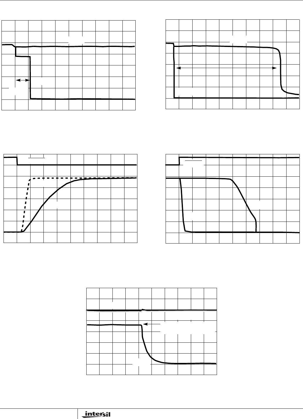
The primary function of any OC protection device is to
quickly isolate the voltage bus from a faulty load. Unlike the
PPTC and other vendor available IC products, the ISL6119
internal timer that starts upon OC detection provides
consistent protection that is not temperature dependent. See
Figures 14 and 15 for a comparison of the time to protection
offered by the ISL6119 vs the PPTC. Figure 14 illustrates the
ISL6119 timed latch-off of 12ms with a 1.5A load and
Figure 15 shows the 8 second latch-off of the PPTC at
approximately its trip current rating of 1.5A.
Using the ISL6119USBEVAL1 Platform
General and Biasing Information
The ISL6119USBEVAL1 platform, Figure 20, allows
evaluation of the ISL6119 dual power supply control IC in a
USB environment.
The evaluation platform is biased and monitored through
numerous test points (TP#). See Table 2 for test point
assignments and descriptions.
Upon proper bias the ISL6119L is held off through pull up
resistors on the enable pins and is enabled by signaling
either or both of the ISL6119L switches TP3, and/or TP4 low
(<0.6V).
The USB connector is provided so that either test loads or
USB peripherals can be powered. In addition, differential
signalling (D+ and D-) access points are provided for each
output port so that I/O activity can also be conducted in a
prototype environment.
TABLE 1. ISL6119EVAL1 TEST POINT ASSIGNMENTS
TP # DESCRIPTION
TP1 Eval Board and IC Gnd
TP2 Eval Bd +5V Bias
TP3 Enable Switch 1
TP4 Enable Switch 2
TP5 Switch 2 Fault
TP6 Switch Out 2
TP7 Switch Out 1
TP8 Switch 1 Fault
TP9 IC VIN Pin
TP10 PPTC Load Side
TP11 Invoke Over Current
TABLE 2. ISL6119USBEVAL1 TEST POINT ASSIGNMENTS
TP # DESCRIPTION
TP1 Eval Board and IC Gnd
TP2 Eval Bd +5V Bias
TP3 Enable Switch 1
TP4 Enable Switch 2
TP5 Switch 1 Fault
TP8 Switch 2 Fault
ISL6119