General Description
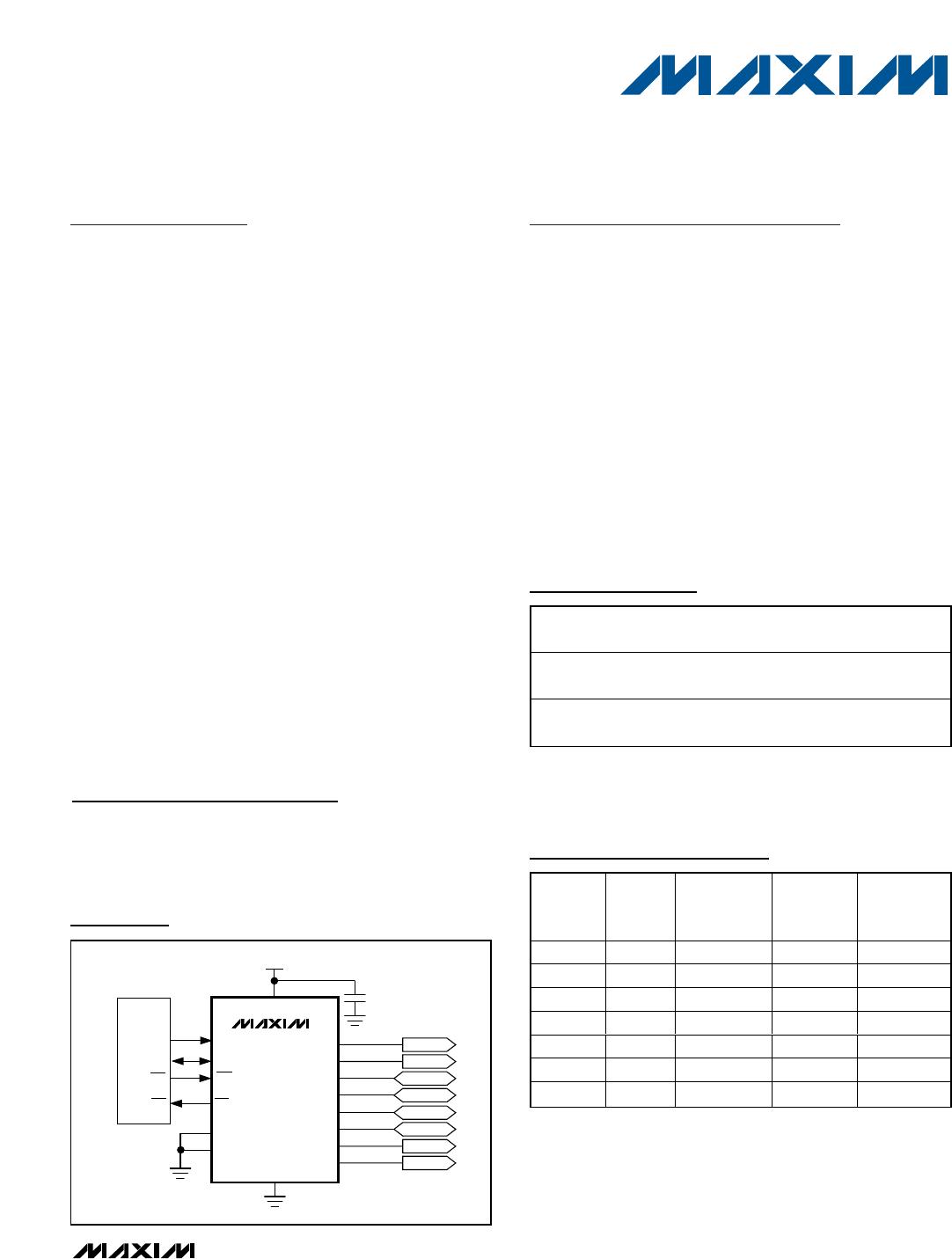
The MAX7323 2-wire serial-interfaced peripheral features
eight I/O ports. Four ports are push-pull outputs and the
other four are open-drain I/O ports that are overvoltage
protected up to +6V independent of the supply voltage.
The four I/O ports configured as inputs are continu-
ously monitored for state changes (transition detec-
tion). State changes are indicated by the open-drain
INT output. The interrupt is latched, allowing detection
of transient changes. When the MAX7323 is subse-
quently accessed through the serial interface, any
pending interrupt is cleared.
The four push-pull and four open-drain outputs are
rated to sink 20mA and are capable of driving LEDs.
The RST input clears the serial interface, terminating
any I
2
C communication to or from the MAX7323.
The MAX7323 uses two address inputs with four-level
logic to allow 16 I
2
C slave addresses. The slave
address also determines the power-up logic state for
the I/O ports, and enables or disables internal 40kΩ
pullups for the input ports in groups of two ports.
The MAX7323 is one device in a family of pin-compatible
port expanders with a choice of input ports, open-drain
I/O ports, and push-pull output ports (see Table 1).
The MAX7323 is available in 16-pin QSOP and 16-pin
TQFN packages, and is specified over the automotive
temperature range (-40°C to +125°C).
Features
400kHz I
2
C Serial Interface
+1.71V to +5.5V Operating Voltage
4 Push-Pull Output Ports Rated at 20mA Sink
Current
4 Open-Drain I/O Ports Rated to 20mA Sink Current
4 I/O Ports Are Overvoltage Protected to +6V
Transient Changes Are Latched, Allowing Detection
Between Read Operations
INT Output Alerts Change on Inputs
AD0 and AD2 Inputs Select from 16 Slave
Addresses
Low 0.6µA (typ) Standby Current
-40°C to +125°C Operating Temperature Range
MAX7323
I
2
C Port Expander with 4 Push-Pull Outputs
and 4 Open-Drain I/Os
________________________________________________________________ Maxim Integrated Products 1
19-3806; Rev 1; 7/07
For pricing, delivery, and ordering information, please contact Maxim Direct at 1-888-629-4642,
or visit Maxim’s website at www.maxim-ic.com.
Ordering Information
PART
TEMP
RANGE
PIN-
PACKAGE
TOP
MARK
PKG
CODE
MAX7323AEE+
-40°C to
+125°C
16 QSOP E16-4
MAX7323ATE+
-40°C to
+125°C
16 TQFN-EP*
3mm x 3mm
ADE T1633-4
Pin Configurations and Functional Diagram appear at end
of data sheet.
Selector Guide
PART INPUTS
INTERRUPT
MASK
OPEN-
DRAIN
OUTPUTS
PUSH-PULL
OUTPUTS
MAX7319 8 Yes
MAX7320 8
MAX7321 Up to 8 Up to 8
MAX7322 4 Yes 4
MAX7323 Up to 4 Up to 4 4
MAX7328 Up to 8 Up to 8
MAX7329 Up to 8 Up to 8
+Denotes a lead-free package.
*EP = Exposed paddle.
Cell Phones
SAN/NAS
Servers
Notebooks
RAID
Automotive
Applications
MAX7323
P2
O7
O6
P5
P4
V+
0.047μF
μC
SCL
SDA
SCL
AD0
O1
O0
SDA
P3
AD2
INT
OUTPUT
OUTPUT
RST
INT
RST
I/O
I/O
I/O
I/O
OUTPUT
OUTPUT
3.3V
GND
Typical Application Circuit
MAX7323
I
2
C Port Expander with 4 Push-Pull Outputs
and 4 Open-Drain I/Os
2 _______________________________________________________________________________________
ABSOLUTE MAXIMUM RATINGS
Stresses beyond those listed under “Absolute Maximum Ratings” may cause permanent damage to the device. These are stress ratings only, and functional
operation of the device at these or any other conditions beyond those indicated in the operational sections of the specifications is not implied. Exposure to
absolute maximum rating conditions for extended periods may affect device reliability.
(All voltages referenced to GND.)
Supply Voltage V+....................................................-0.3V to +6V
SCL, SDA, AD0, AD2, RST, INT, P2–P5 ...................-0.3V to +6V
O0, O1, O6, O7...............................................-0.3 to (V+ + 0.3V)
O0, O1, O6, O7 Output Current........................................±25mA
P2–P5 Sink Current...........................................................±25mA
SDA Sink Current ............................................................... 10mA
INT Sink Current..................................................................10mA
Total V+ Current..................................................................50mA
Total GND Current ...........................................................100mA
Continuous Power Dissipation (T
A
= +70°C)
16-Pin QSOP (derate 8.3mW/°C above +70°C)...........667mW
16-Pin TQFN (derate 15.6mW/°C above +70°C) .......1250mW
Operating Temperature Range .........................-40°C to +125°C
Junction Temperature......................................................+150°C
Storage Temperature Range .............................-65°C to +150°C
Lead Temperature (soldering, 10s) .................................+300°C
ELECTRICAL CHARACTERISTICS
(V+ = +1.71V to +5.5V, T
A
= -40°C to +125°C, unless otherwise noted. Typical values are at V+ = +3.3V, T
A
= +25°C.) (Note 1)
PARAMETER SYMBOL CONDITIONS MIN TYP MAX UNITS
Operating Supply Voltage V+ 1.71 5.50 V
Power-On Reset Voltage V
POR
V+ falling 1.6 V
Standby Current
(Interface Idle)
I
STB
SCL and SDA and other digital inputs at V+ 0.6 1.5 µA
Supply Current
(Interface Running)
I+ f
SCL
= 400kHz; other digital inputs at V+ 23 55 µA
V+ 1.8V 0.8 x V+
Input High Voltage
SDA, SCL, AD0, AD2, RST, P2–P5
V
IH
V+ 1.8 0.7 x V+
V
V+ 1.8V 0.2 x V+
Input Low Voltage
SDA, SCL, AD0, AD2, RST, P2–P5
V
IL
V+ 1.8V 0.3 x V+
V
Input Leakage Current
SDA, SCL, AD0, AD2, RST, P2–P5
I
IH
, I
IL
SDA, SCL, AD0, AD2, RST, P2–P5 at V+ or
GND, internal pullup disabled
-0.2 +0.2 µA
Input Capacitance
SDA, SCL, AD0, AD2, RST, P2–P5
10 pF
V+ = +1.71V, I
SINK
= 5mA 105 180
V+ = +2.5V, I
SINK
= 10mA 131 240
V+ = +3.3V, I
SINK
= 15mA 154 290
Output Low Voltage
O0, O1, O6, O7, P2–P5
V
OL
V+ = +5V, I
SINK
= 20mA 160 310
mV
V+ = +1.71V, I
SOURCE
= 2mA V+ - 250 V + - 30
V+ = +2.5V, I
SOURCE
= 5mA V+ - 360 V + - 70
V+ = +3.3V, I
SOURCE
= 5mA V+ - 260 V + - 100
Output High Voltage
O0, O1, O6, O7
V
OH
V+ = +5V, I
SOURCE
= 10mA V+ - 350 V + - 120
mV
Output Low Voltage
SDA
V
OLSDA
I
SINK
= 6mA 250 mV
Output Low Voltage
INT
V
OLINT
I
SINK
= 5mA 130 250 mV
Port Input Pullup Resistor R
PU
25 40 55 kΩ
MAX7323
I
2
C Port Expander with 4 Push-Pull Outputs
and 4 Open-Drain I/Os
_______________________________________________________________________________________ 3
PORT AND INTERRUPT INT TIMING CHARACTERISTICS
(V+ = +1.71V to +5.5V, T
A
= -40°C to +125°C, unless otherwise noted. Typical values are at V+ = +3.3V, T
A
= +25°C.) (Note 1)
PARAMETER SYMBOL CONDITIONS MIN TYP MAX UNITS
Port Output Data Valid t
PPV
C
L
100pF 4 µs
Port Input Setup Time t
PSU
C
L
100pF 0 µs
Port Input Hold Time t
PH
C
L
100pF 4 µs
INT Input Data Valid Time t
IV
C
L
100pF 4 µs
INT Reset Delay Time from STOP t
IP
C
L
100pF 4 µs
INT Reset Delay Time from
Acknowledge
t
IR
C
L
100pF 4 µs
TIMING CHARACTERISTICS
(V+ = +1.71V to +5.5V, T
A
= -40°C to +125°C, unless otherwise noted. Typical values are at V+ = +3.3V, T
A
= +25°C.) (Note 1)
PARAMETER SYMBOL CONDITIONS MIN TYP MAX UNITS
Serial-Clock Frequency f
SCL
400 kHz
Bus Free Time Between a STOP
and a START Condition
t
BUF
1.3 µs
Hold Time (Repeated) START
Condition
t
HD
,
STA
0.6 µs
Repeated START Condition
Setup Time
t
SU
,
STA
0.6 µs
STOP Condition Setup Time t
SU
,
STO
0.6 µs
Data Hold Time t
HD
,
DAT
(Note 2) 0.9 µs
Data Setup Time t
SU
,
DAT
100 ns
SCL Clock Low Period t
LOW
1.3 µs
SCL Clock High Period t
HIGH
0.7 µs
Rise Time of Both SDA and SCL
Signals, Receiving
t
R
(Notes 3, 4)
20 +
0.1C
b
300 ns
Fall Time of Both SDA and SCL
Signals, Receiving
t
F
(Notes 3, 4)
20 +
0.1C
b
300 ns
Fall Time of SDA, Transmitting t
F,TX
(Notes 3, 4)
20 +
0.1C
b
250 ns
Pulse Width of Spike Suppressed t
SP
(Note 5) 50 ns
Capacitive Load for Each Bus
Line
C
b
(Note 3) 400 pF
RST Pulse Width t
W
500 ns
RST Rising to START Condition
Setup Time
t
RST
s
Note 1: All parameters tested at T
A
= +25°C. Specifications over temperature are guaranteed by design.
Note 2: A master device must provide a hold time of at least 300ns for the SDA signal (referred to V
IL
of the SCL signal) in order to
bridge the undefined region of SCL’s falling edge.
Note 3: Guaranteed by design.
Note 4: C
b
= total capacitance of one bus line in pF. t
R
and t
F
measured between 0.3 x V+ and 0.7 x V+ with I
SINK
6mA.
Note 5: Input filters on the SDA and SCL inputs suppress noise spikes less than 50ns.

MAX7323ATE+

Mfr. #:
Manufacturer:
Maxim Integrated
Description:
Interface - I/O Expanders I2C Port Expander w/4 P-P Out & 4 I/O
Lifecycle:
New from this manufacturer.
Delivery:
DHL FedEx Ups TNT EMS
Payment:
T/T Paypal Visa MoneyGram Western Union

Products related to this Datasheet