1
3MHz Dual 1500mA Step-Down Converters and Dual
Low-Input LDOs
ISL9307
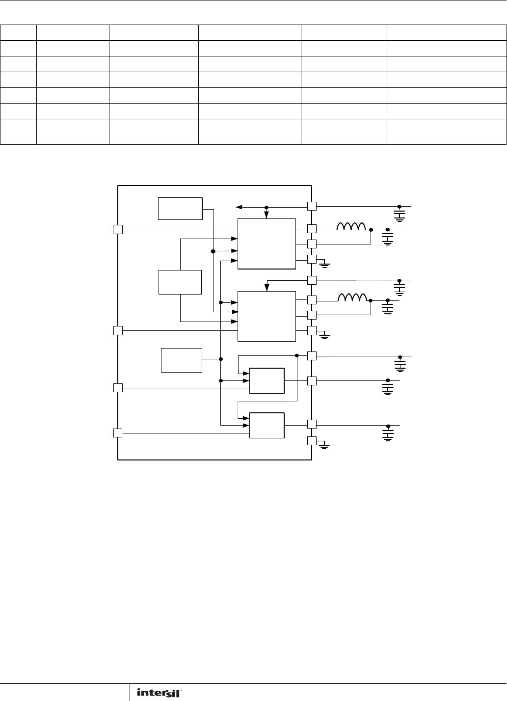
The ISL9307 is an integrated mini Power Management IC
(mini-PMIC) ideal for applications for powering low-voltage
microprocessor or multiple voltage rails with a battery as an
input source, such as a single Li-ion or Li-polymer. ISL9307
integrates two high-efficiency, 3MHz, synchronous step-down
converters (DCD1 and DCD2) and two low-input, low-dropout
linear regulators (LDO1 and LDO2).
The 3MHz PWM switching frequency allows the use of very
small external inductors and capacitors. Both step-down
converters can enter skip mode under light load conditions to
further improve efficiency and maximize battery life.
The ISL9307 features EN pins for each channel, thus allowing
startup delay for power sequencing.
The ISL9307 also provides two 300mA low-dropout (LDO)
regulators. The input voltage range is 1.5V to 5.5V, which
allows them to be powered from one of the on-chip step-down
converters or directly from a battery. The default LDO power-up
output comes with factory pre-set fixed output voltage options
between 0.9V and 3.3V.
The ISL9307 is available in a 4mmx4mm 16 Ld TQFN.
Features
• Dual 1500mA, Synchronous Step-down Converters and Dual
300mA, General-purpose LDOs
• Input Voltage Range
- DCD1/DCD2 . . . . . . . . . . . . . . . . . . . . . . . . . . . . 2.5V to 5.5V
- VINLDO . . . . . . . . . . . . . . . . . . . . . . . . . . . . . . . . 1.5V to 5.5V
• Adjustable Output Voltage
- VODCD1/VODCD2 . . . . . . . . . . . . . . . . . . . . . . . . 0.8V to V
IN
•50μA I
Q
(Typ) with DCD1/DCD2 in Skip Mode; 20μA I
Q
(Typ)
for each Enabled LDO
• EN Pins for DCD1/DCD2 and LDO1/LDO2
• Small, Thin, 4mmx4mm TQFN
Applications
• Cellular Phones, Smart Phones
• PDAs, Portable Media Players, Portable Instruments
• Single Li-ion/Li-polymer Battery-Powered Equipment
•DSP Core Power
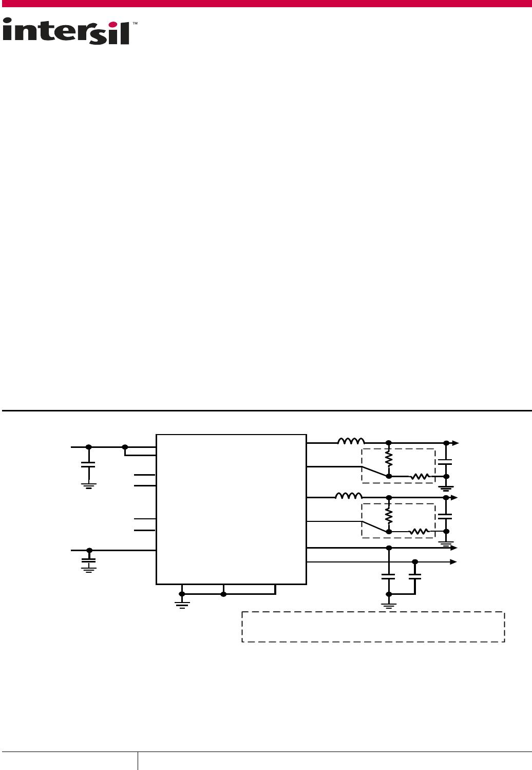
FIGURE 1. TYPICAL APPLICATION DIAGRAM
ISL9307
L
1
= 1.5µH
2.5V TO 5.5V
1500mA
1500mA
1.5V TO 5.5V
300mA
300mA
R
1
R
2
R
3
R
4
1µF
C
2
L
2
= 1.5µH
C
4
10µF
C
5
10µF
C
6
1µF
C
7
1µF
ENDCD1
VINDCD1
VINLDO
VINDCD2
ENDCD2
ENLDO1
ENLDO2
GNDDCD1 GNDDCD2 GNDLDO
C
1
10µF
VOLDO2
SW1
FB1
SW2
FB2
VOLDO1
NOTE: ONLY FOR ADJUSTABLE OUTPUT VERSION. FOR FIXED
OUTPUT VERSION, DIRECTLY CONNECT THE FB PIN TO THE
OUTPUT OF THE BUCK CONVERTER.
CAUTION: These devices are sensitive to electrostatic discharge; follow proper IC Handling Procedures.
1-888-INTERSIL or 1-888-468-3774
| Copyright Intersil Americas Inc. 2012. All Rights Reserved
Intersil (and design) is a trademark owned by Intersil Corporation or one of its subsidiaries.
All other trademarks mentioned are the property of their respective owners.
September 20, 2012
FN7931.3