ISL9307
8
FN7931.3
September 20, 2012
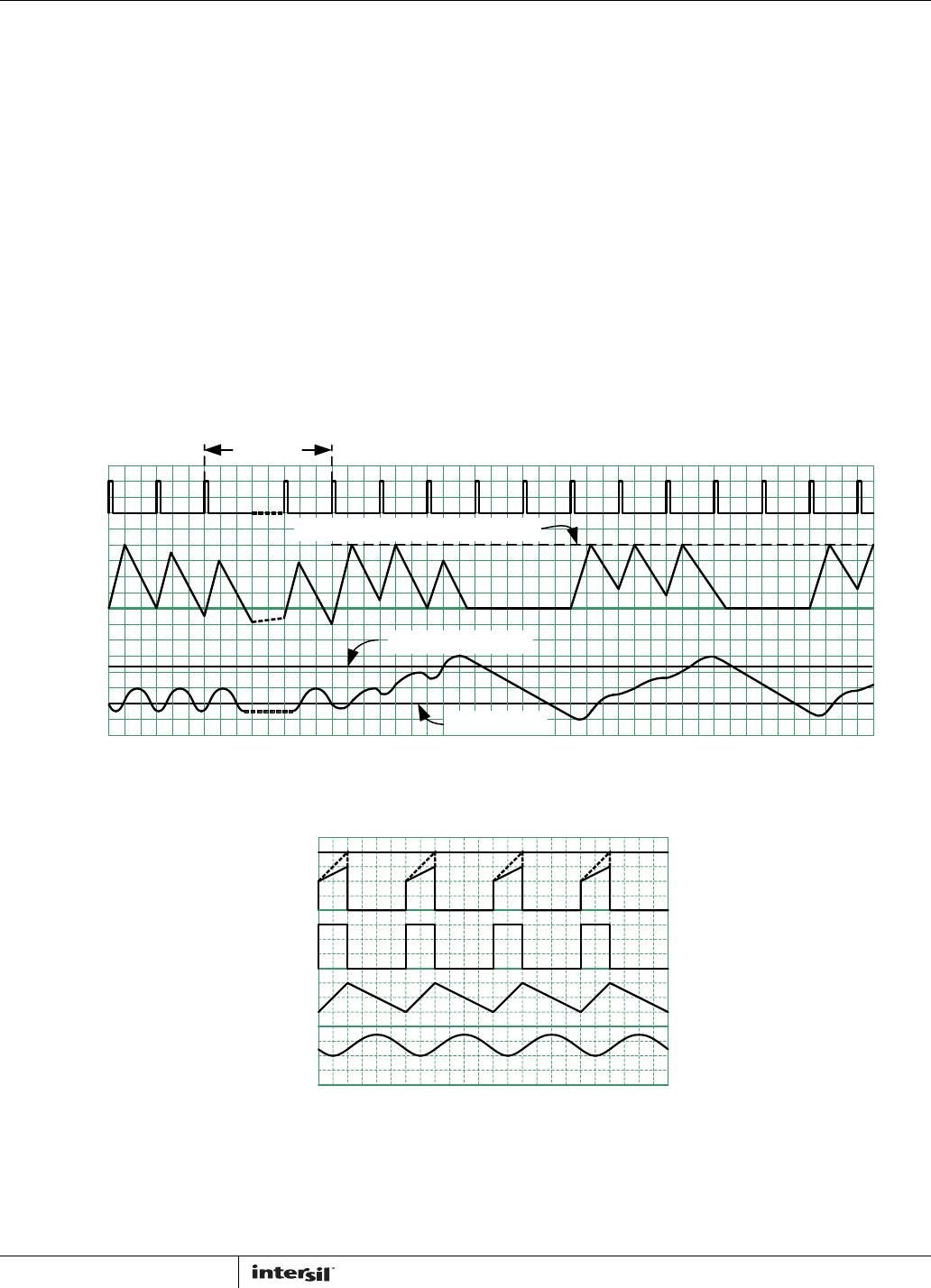
Soft-Start
Soft-start reduces the in-rush current during the start-up stage. The
soft-start block limits the current rising speed so that the output
voltage rises in a controlled fashion.
Overcurrent Protection
The ISL9307 provides overcurrent protection for DCD1 and DCD2 for
when an overload condition occurs. When the current at P-channel
MOSFET is sensed to reach the current limit, the internal
protection circuit is triggered to turn off the P-channel MOSFET
immediately.
DCD Short-Circuit Protection
The ISL9307 provides short-circuit protection for both DCD1 and
DCD2. The feedback voltage is monitored for output short-circuit
protection. When the output voltage is sensed to be lower than a
certain threshold, the internal circuit will change the PWM
oscillator frequency to a lower frequenciy to protect the IC from
damage. The P-channel MOSFET peak current limit remains
active during this state.
Undervoltage Lockout (UVLO)
An undervoltage lockout (UVLO) circuit is provided on ISL9307.
The UVLO circuit block can prevent abnormal operation in the
event that the supply voltage is too low to guarantee proper
operation. The UVLO on VINDCD1 is set for a typical 2.2V with
100mV hysteresis. VINLDO is set for a typical 1.4V with 50mV
hysteresis. When the input voltage is sensed to be lower than the
UVLO threshold, the related channel is disabled.
Low Dropout Operation
Both DCD1 and DCD2 converters feature low dropout operation
to maximize battery life. When the input voltage drops to a level
at which the converter can no longer operate under switching
regulation to maintain the output voltage, the P-channel MOSFET
is completely turned on (100% duty cycle). The dropout voltage
under such a condition is the product of the load current and the
ON-resistance of the P-channel MOSFET. Minimum required input
voltage (V
IN
) under such a condition is the sum of output voltage
plus voltage drop across the inductor and the P-channel MOSFET
switch.
Active Output Voltage Discharge For DCD1,
DCD2
The ISL9307 offers a feature to actively discharge the output
voltage of DCD1 and DCD2 via an internal bleeding resistor
(typical 115Ω) when the channel is disabled.
Thermal Shutdown
The ISL9307 provides a built-in thermal protection function with
thermal shutdown threshold temperature set at +155°C with
+25°C hysteresis (typical). When the die temperature is sensed
to reach +155°C, the regulator is completely shut down, and as
the temperature is sensed to drop to +130°C (typical), the device
resumes normal operation, starting from soft-start.
Board Layout Recommendations
The ISL9307 is a high frequency switching charger and hence the
PCB layout is a very important design practice to ensure a
satisfactory performance.
The power loop is composed of the output inductor, L; the output
capacitor, C
OUT
; the SW pin; and the PGND pin. It is important to
make the power loop as small as possible, and the connecting
traces among them should be direct, short and wide. The same
practice should be applied to the connection of the VIN pin; the
input capacitor, C
IN
; and PGND.
The switching node of the converter, the SW pin, and the traces
connected to this node are very noisy, so keep the voltage
feedback trace and other noise-sensitive traces away from these
noisy traces.
The input capacitor should be placed as close as possible to the
VIN pin. The ground of the input and output capacitors should be
connected as close as possible as well. In addition, a solid ground
plane is helpful for good EMI performance.
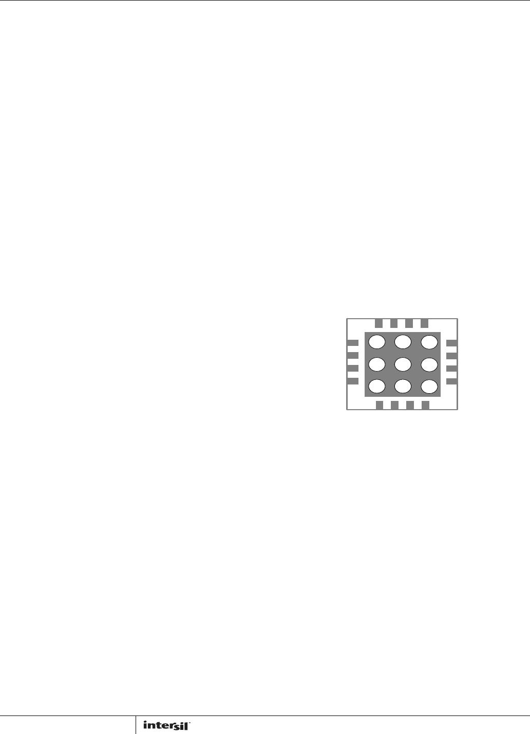
The ISL9307 employs a thermally enhanced TQFN package with
an exposed pad. The exposed pad should be properly soldered
onto the thermal pad of the board to remove heat from the IC.
The thermal pad should be big enough for nine vias, as shown in
Figure 4.
FIGURE 4. EXPOSED THERMAL PAD