ESD7361P2T5G

© Semiconductor Components Industries, LLC, 2016
November, 2016 − Rev. 3
1 Publication Order Number:
ESD7361/D
ESD7361, SZESD7361
ESD Protection Diodes
Low Capacitance ESD Protection Diode
for High Speed Data Line
The ESD7361 Series ESD protection diodes are designed to protect
high speed data lines from ESD. Ultra−low capacitance make this
device an ideal solution for protecting voltage sensitive high speed
data lines.
Features
Low Capacitance (0.55 pF Max, I/O to GND)
Protection for the Following IEC Standards:
IEC61000−4−2 (ESD): Level 4 ±15 kV Contact
IEC61000−4−4 (EFT): 40 A −5/50 ns
IEC61000−4−5 (Lightning): 1 A (8/20 ms)
ISO 10605 (ESD) 330 pF/2 kW ±15 kV Contact
SZ Prefix for Automotive and Other Applications Requiring Unique
Site and Control Change Requirements; AEC−Q101 Qualified and
PPAP Capable
These Devices are Pb−Free, Halogen Free/BFR Free and are RoHS
Compliant
Typical Applications
Wireless Charger
Near Field Communications
MAXIMUM RATINGS (T
J
= 25°C unless otherwise noted)
Rating
Symbol Value Unit
Operating Junction Temperature Range T
J
55 to +125 °C
Storage Temperature Range T
stg
55 to +150 °C
Lead Solder Temperature −
Maximum (10 Seconds)
T
L
260 °C
IEC 61000−4−2 Contact (ESD)
IEC 61000−4−2 Air (ESD)
ISO 10605 330 pF/2 kW Contact (ESD)
ESD
ESD
ESD
±15
±15
±15
kV
kV
kV
Stresses exceeding those listed in the Maximum Ratings table may damage the
device. If any of these limits are exceeded, device functionality should not be
assumed, damage may occur and reliability may be affected.
MARKING
DIAGRAMS
PIN CONFIGURATION
AND SCHEMATIC
www.
onsemi.com
X, XX = Specific Device Code
M = Date Code
1
Cathode
2
Anode
SOD−323
CASE 477
SOD−523
CASE 502
SOD−923
CASE 514AB
1
2
7H
M
1
2
7X
12
M
2 M
See detailed ordering and shipping information on page 6 o
f
this data sheet.
ORDERING INFORMATION
ESD7361, SZESD7361
www.onsemi.com
2
ELECTRICAL CHARACTERISTICS
(T
A
= 25°C unless otherwise noted)
Symbol
Parameter
I
PP
Maximum Reverse Peak Pulse Current
V
C
Clamping Voltage @ I
PP
V
RWM
Working Peak Reverse Voltage
I
R
Maximum Reverse Leakage Current @ V
RWM
V
BR
Breakdown Voltage @ I
T
I
T
Test Current
*See Application Note AND8308/D for detailed explanations of
datasheet parameters.
Uni−Directional TVS
I
PP
I
F
V
I
I
R
I
T
V
RWM
V
C
V
BR
V
F
ELECTRICAL CHARACTERISTICS (T
A
= 25°C unless otherwise specified)
Parameter
Symbol Conditions Min Typ Max Unit
Reverse Working Voltage V
RWM
5 16 V
Breakdown Voltage V
BR
I
T
= 1 mA; pin 1 to pin 2 16.5 V
Reverse Leakage Current I
R
V
RWM
= 5.0 V
V
RWM
= 15 V
<1
20
1000
1000
nA
nA
Clamping Voltage (Note 2) V
C
I
PP
= 8 A 31 V
Clamping Voltage (Note 2) V
C
I
PP
= 16 A 34 V
Junction Capacitance C
J
V
R
= 0 V, f = 1 MHz
V
R
= 0 V, f < 1 GHz
0.55
0.55
pF
Dynamic Resistance R
DYN
TLP Pulse 0.735
W
Insertion Loss f = 1 MHz
f = 5 GHz
0.01
2
dB
Product parametric performance is indicated in the Electrical Characteristics for the listed test conditions, unless otherwise noted. Product
performance may not be indicated by the Electrical Characteristics if operated under different conditions.
1. For test procedure see Figures 9 and 10 and application note AND8307/D.
2. ANSI/ESD STM5.5.1 − Electrostatic Discharge Sensitivity Testing using Transmission Line Pulse (TLP) Model.
TLP conditions: Z
0
= 50 W, t
p
= 100 ns, t
r
= 4 ns, averaging window; t
1
= 30 ns to t
2
= 60 ns.
Figure 1. Typical IV Characteristics Figure 2. Typical CV Characteristics
1.E−03
1.E−04
1.E−05
1.E−06
1.E−07
1.E−08
1.E−09
1.E−10
1.E−11
1.E−12
1.E−13
0 5 10 15 20 25 30
VOLTAGE (V)
CURRENT (A)
V
Bias
(V)
CAPACITANCE (pF)
1
0.8
0.6
0.4
0.2
0
04
8
14 182
61012
16
ESD7361, SZESD7361
www.onsemi.com
3
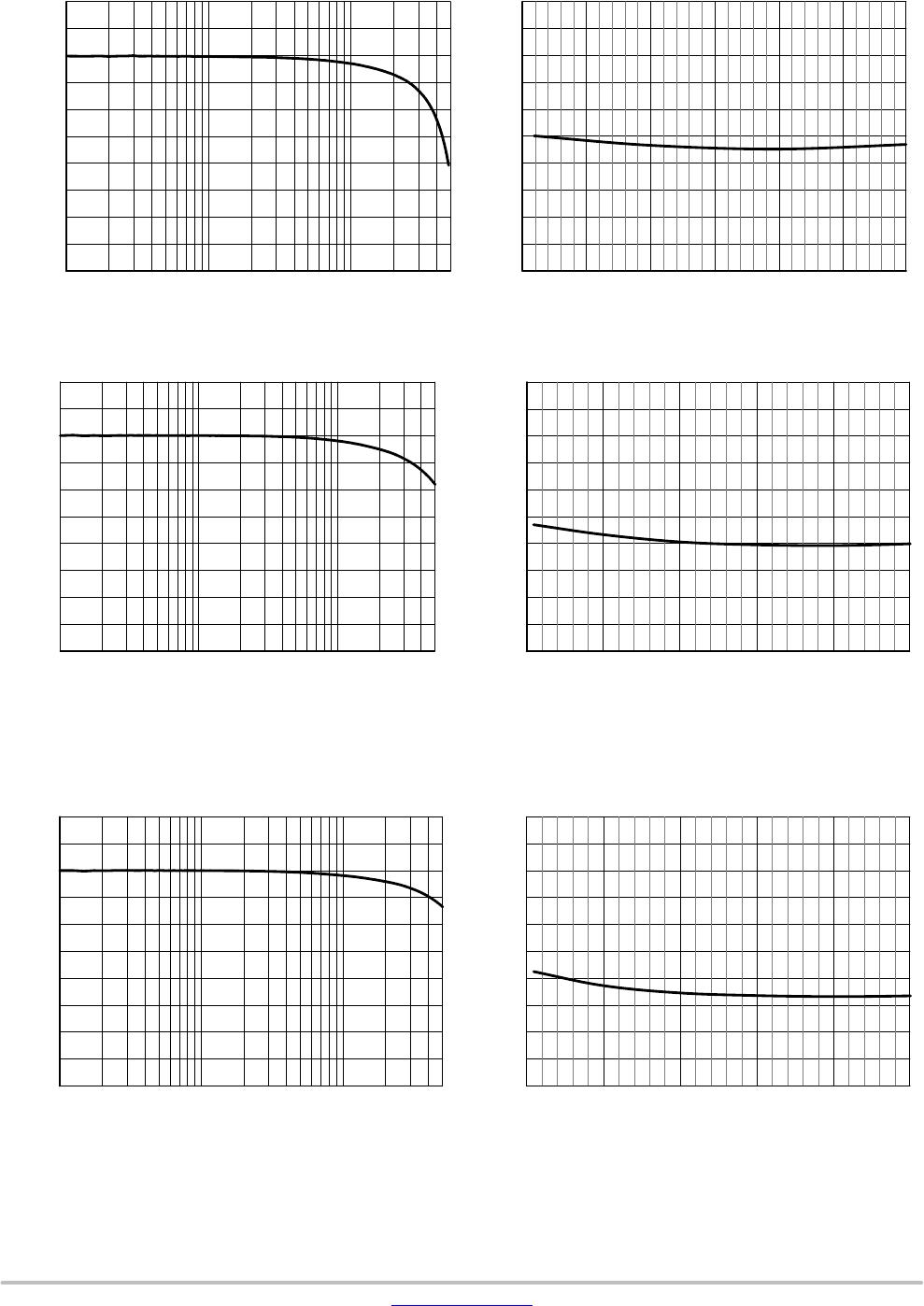
Figure 3. Typical Insertion Loss
ESD7361HT1G (SOD323)
Figure 4. Typical Capacitance Over Frequency
ESD7361HT1G (SOD323)
S21 (dB)
FREQUENCY (Hz)
CAPACITANCE (pF)
FREQUENCY (Hz)
1
1.E+07 1.E+08 1.E+09
1
1.E+07 5.E+08 1.E+09 2.E+09 2.E+09 3.E+09
Figure 5. Typical Insertion Loss
ESD7361XV2T1G (SOD523)
Figure 6. Typical Capacitance Over Frequency
ESD7361XV2T1G (SOD523)
CAPACITANCE (pF)
FREQUENCY (Hz)
S21 (dB)
FREQUENCY (Hz)
1.E+07 1.E+08 1.E+09
1
1
1.E+07
Figure 7. Typical Insertion Loss
ESD7361P2T5G (SOD923)
S21 (dB)
FREQUENCY (Hz)
Figure 8. Typical Capacitance Over Frequency
ESD7361P2T5G (SOD923)
CURRENT (A)
FREQUENCY (Hz)
0.5
0
−0.5
−1
−1.5
−2
−2.5
−3
−3.5
−4
0.9
0.8
0.7
0.6
0.5
0.4
0.3
0.2
0.1
0
0.5
0
−0.5
−1
−1.5
−2
−2.5
−3
−3.5
−4
1
1.E+07 1.E+09 2.E+09 3.E+09
0.9
0.8
0.7
0.6
0.5
0.4
0.3
0.2
0.1
0
4.E+09
0.5
0
−0.5
−1
−1.5
−2
−2.5
−3
−3.5
−4
1.E+08 1.E+09
1
0.9
0.8
0.7
0.6
0.5
0.4
0.3
0.2
0.1
0
1.E+07 1.E+09 2.E+09 3.E+09 4.E+09

ESD7361P2T5G

Mfr. #:
Manufacturer:
ON Semiconductor
Description:
ESD Suppressors / TVS Diodes 16V ESD PROTECTION
Lifecycle:
New from this manufacturer.
Delivery:
DHL FedEx Ups TNT EMS
Payment:
T/T Paypal Visa MoneyGram Western Union