ESD7361P2T5G

ESD7361, SZESD7361
www.onsemi.com
4
IEC 61000−4−2 Spec.
Level
Test Volt-
age (kV)
First Peak
Current
(A)
Current at
30 ns (A)
Current at
60 ns (A)
1 2 7.5 4 2
2 4 15 8 4
3 6 22.5 12 6
4 8 30 16 8
I
peak
90%
10%
IEC61000−4−2 Waveform
100%
I @ 30 ns
I @ 60 ns
t
P
= 0.7 ns to 1 ns
Figure 9. IEC61000−4−2 Spec
Figure 10. Diagram of ESD Clamping Voltage Test Setup
50 W
50 W
Cable
TVS
Oscilloscope
ESD Gun
The following is taken from Application Note
AND8308/D − Interpretation of Datasheet Parameters
for ESD Devices.
ESD Voltage Clamping
For sensitive circuit elements it is important to limit the
voltage that an IC will be exposed to during an ESD event
to as low a voltage as possible. The ESD clamping voltage
is the voltage drop across the ESD protection diode during
an ESD event per the IEC61000−4−2 waveform. Since the
IEC61000−4−2 was written as a pass/fail spec for larger
systems such as cell phones or laptop computers it is not
clearly defined in the spec how to specify a clamping voltage
at the device level. ON Semiconductor has developed a way
to examine the entire voltage waveform across the ESD
protection diode over the time domain of an ESD pulse in the
form of an oscilloscope screenshot, which can be found on
the datasheets for all ESD protection diodes. For more
information on how ON Semiconductor creates these
screenshots and how to interpret them please refer to
AND8307/D.
ESD7361, SZESD7361
www.onsemi.com
5
Figure 11. Positive TLP I−V Curve
Figure 12. Negative TLP I−V Curve
TLP CURRENT (A)
V
C
, VOLTAGE (V)
25
040353051015 2520
TLP CURRENT (A)
V
C
, VOLTAGE (V)
−25
0 −14−12−10−2 −4 −6 −8
NOTE: TLP parameter: Z
0
= 50 W, t
p
= 100 ns, t
r
= 300 ps, averaging window: t
1
= 30 ns to t
2
= 60 ns. V
IEC
is the equivalent voltage
stress level calculated at the secondary peak of the IEC 61000−4−2 waveform at t = 30 ns with 2 A/kV. See TLP description
below for more information.
20
15
10
5
0
−20
−15
−10
−5
0
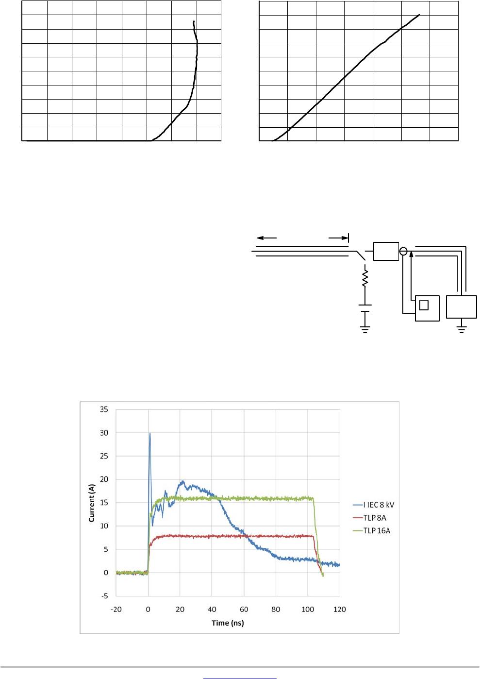
Transmission Line Pulse (TLP) Measurement
Transmission Line Pulse (TLP) provides current versus
voltage (I−V) curves in which each data point is obtained
from a 100 ns long rectangular pulse from a charged
transmission line. A simplified schematic of a typical TLP
system is shown in Figure 13. TLP I−V curves of ESD
protection devices accurately demonstrate the product’s
ESD capability because the 10s of amps current levels and
under 100 ns time scale match those of an ESD event. This
is illustrated in Figure 14 where an 8 kV IEC 61000−4−2
current waveform is compared with TLP current pulses at
8 A and 16 A. A TLP I−V curve shows the voltage at which
the device turns on as well as how well the device clamps
voltage over a range of current levels.
Figure 13. Simplified Schematic of a Typical TLP
System
DUT
L
S
÷
Oscilloscope
Attenuator
10 MW
V
C
V
M
I
M
50 W Coax
Cable
50 W Coax
Cable
Figure 14. Comparison Between 8 kV IEC 61000−4−2 and 8 A and 16 A TLP Waveforms
ESD7361, SZESD7361
www.onsemi.com
6
ORDERING INFORMATION
Device Package Shipping
ESD7361HT1G SOD−323
(Pb−Free)
3000 / Tape & Reel
ESD7361XV2T1G SOD−523
(Pb−Free)
3000 / Tape & Reel
ESD7361P2T5G SOD−923
(Pb−Free)
8000 / Tape & Reel
SZESD7361HT1G SOD−323
(Pb−Free)
3000 / Tape & Reel
SZESD7361XV2T1G SOD−523
(Pb−Free)
3000 / Tape & Reel
SZESD7361P2T5G SOD−923
(Pb−Free)
8000 / Tape & Reel
For information on tape and reel specifications, including part orientation and tape sizes, please refer to our Tape and Reel Packaging
Specifications Brochure, BRD8011/D.

ESD7361P2T5G

Mfr. #:
Manufacturer:
ON Semiconductor
Description:
ESD Suppressors / TVS Diodes 16V ESD PROTECTION
Lifecycle:
New from this manufacturer.
Delivery:
DHL FedEx Ups TNT EMS
Payment:
T/T Paypal Visa MoneyGram Western Union