OP27 Data Sheet
Rev. H | Page 14 of 21
APPLICATIONS INFORMATION
OP27 series units can be inserted directly into OP07 sockets
with or without removal of external compensation or nulling
components.
OP27 offset voltage can be nulled to 0 (or another
desired setting) using a potentiometer (see Figure 35).
The
OP27 provides stable operation with load capacitances of
up to 2000 pF and ±10 V swings; larger capacitances should be
decoupled with a 50 Ω resistor inside the feedback loop. The
OP27 is unity-gain stable.
Thermoelectric voltages generated by dissimilar metals at the
input terminal contacts can degrade the drift performance.
Best operation is obtained when both input contacts are
maintained at the same temperature.
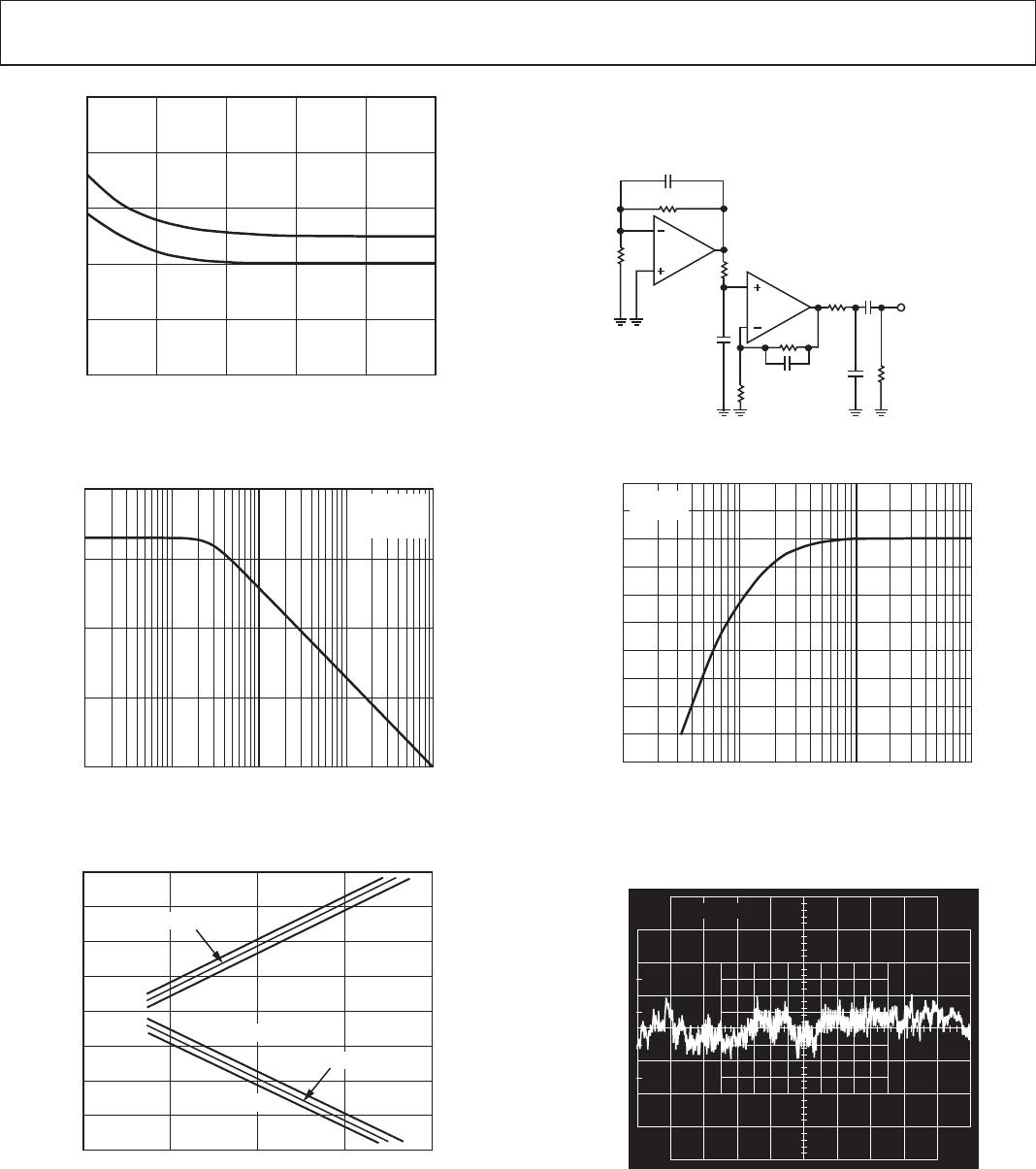
Figure 35. Offset Nulling Circuit
OFFSET VOLTAGE ADJUSTMENT
The input offset voltage of the OP27 is trimmed at wafer level.
However, if further adjustment of V
OS
is necessary, a 10 kΩ trim
potentiometer can be used. TCV
OS
is not degraded (see Figure 35).
Other potentiometer values from 1 kΩ to 1 MΩ can be used
with a slight degradation (0.1 µV/°C to 0.2 µV/°C) of TCV
OS
.
Trimming to a value other than zero creates a drift of approxi-
mately (V
OS
/300) µV/°C. For example, the change in TCV
OS
is
0.33 µV/°C if V
OS
is adjusted to 100 µV. The offset voltage
adjustment range with a 10 kΩ potentiometer is ±4 mV. If smaller
adjustment range is required, the nulling sensitivity can be
reduced by using a smaller potentiometer in conjunction with
fixed resistors. For example, Figure 36 shows a network that has
a ±280 µV adjustment range.
Figure 36. Offset Voltage Adjustment
NOISE MEASUREMENTS
To measure the 80 nV p-p noise specification of the OP27 in
the 0.1 Hz to 10 Hz range, the following precautions must be
observed:
x The device must be warmed up for at least five minutes.
As shown in the warm-up drift curve, the offset voltage
typically changes 4 µV due to increasing chip temperature
after power-up. In the 10-second measurement interval,
these temperature-induced effects can exceed tens-of-
nanovolts.
x For similar reasons, the device has to be well-shielded
from air currents. Shielding minimizes thermocouple effects.
x Sudden motion in the vicinity of the device can also
feedthrough to increase the observed noise.
x The test time to measure 0.1 Hz to 10 Hz noise should not
exceed 10 seconds. As shown in the noise-tester frequency
response curve, the 0.1 Hz corner is defined by only one
zero. The test time of 10 seconds acts as an additional zero
to eliminate noise contributions from the frequency band
below 0.1 Hz.
x A noise voltage density test is recommended when
measuring noise on a large number of units. A 10 Hz noise
voltage density measurement correlates well with a 0.1 Hz to
10 Hz p-p noise reading, since both results are determined
by the white noise and the location of the 1/f corner
frequency.
UNITY-GAIN BUFFER APPLICATIONS
When R
f
≤ 100 Ω and the input is driven with a fast, large
signal pulse (>1 V), the output waveform looks as shown in the
pulsed operation diagram (see Figure 37).
During the fast feedthrough-like portion of the output, the
input protection diodes effectively short the output to the input,
and a current, limited only by the output short-circuit protect-
ion, is drawn by the signal generator. With R
f
≥ 500 Ω, the output is
capable of handling the current requirements (I
L
≤ 20 mA at 10 V);
the amplifier stays in its active mode and a smooth transition
occurs.
When R
f
> 2 kΩ, a pole is created with R
f
and the amplifier’s
input capacitance (8 pF) that creates additional phase shift and
reduces phase margin. A small capacitor (20 pF to 50 pF) in
parallel with R
f
eliminates this problem.
+
–
OP27