REV. E
Information furnished by Analog Devices is believed to be accurate and
reliable. However, no responsibility is assumed by Analog Devices for its
use, nor for any infringements of patents or other rights of third parties that
may result from its use. No license is granted by implication or otherwise
under any patent or patent rights of Analog Devices. Trademarks and
registered trademarks are the property of their respective companies.
One Technology Way, P.O. Box 9106, Norwood, MA 02062-9106, U.S.A.
Tel: 781/329-4700 www.analog.com
Fax: 781/326-8703 © 2003 Analog Devices, Inc. All rights reserved.
AD7701
LC
2
MOS
16-Bit A/D Converter
FEATURES
Monolithic 16-Bit ADC
0.0015% Linearity Error
On-Chip Self-Calibration Circuitry
Programmable Low-Pass Filter
0.1 Hz to 10 Hz Corner Frequency
0 V to +2.5 V or 2.5 V Analog Input Range
4 kSPS Output Data Rate
Flexible Serial Interface
Ultralow Power
APPLICATIONS
Industrial Process Control
Weigh Scales
Portable Instrumentation
Remote Data Acquisition
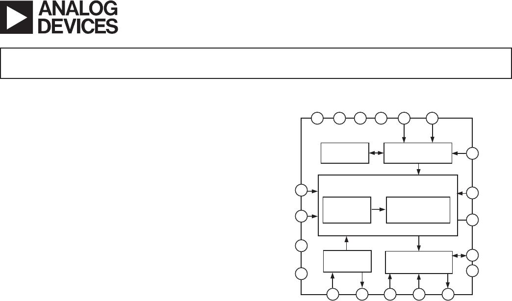
FUNCTIONAL BLOCK DIAGRAM
14 15 7 64 17
AV
DD
DV
DD
AV
SS
DV
SS
SC1 SC2
13
CALIBRATION
SRAM
16-BIT A/D CONVERTER
ANALOG
MODULATOR
CAL
SLEEP
11
20
19
CLOCK
GENERATOR
SERIAL INTERFACE
LOGIC
SDATA
SCLK
3 2 1 18
CLKIN CLKOUT
MODE
DRDY
6-POLE GAUSSIAN
LOW-PASS
DIGITAL FILTER
AD7701
5DGND
AGND
A
IN
V
REF
8
9
10
BP/UP
12
16
CS
CALIBRATION
MICROCONTROLLER
GENERAL DESCRIPTION
The AD7701 is a 16-bit ADC that uses a sigma-delta conversion
technique. The analog input is continuously sampled by an analog
modulator whose mean output duty cycle is proportional to the
input signal. The modulator output is processed by an on-chip
digital filter with a six-pole Gaussian response, which updates
the output data register with 16-bit binary words at word rates up
to 4 kHz. The sampling rate, filter corner frequency, and output
word rate are set by a master clock input that may be supplied
externally, or by a crystal controlled on-chip clock oscillator.
The inherent linearity of the ADC is excellent and endpoint
accuracy is ensured by self-calibration of zero and full scale,
which may be initiated at any time. The self-calibration scheme
can also be extended to null system offset and gain errors in the
input channel.
The output data is accessed through a flexible serial port, which
has an asynchronous mode compatible with UARTs and two
synchronous modes suitable for interfacing to shift registers or
the serial ports of industry-standard microcontrollers.
CMOS construction ensures low power dissipation, and a power-
down mode reduces the idle power consumption to only 10 µW.
PRODUCT HIGHLIGHTS
1. The AD7701 offers 16-bit resolution coupled with outstand-
ing 0.0015% accuracy.
2. No missing codes ensures true, usable, 16-bit dynamic range,
removing the need for programmable gain and level-setting
circuitry.
3. The effects of temperature drift are eliminated by on-chip
self-calibration, which removes zero and gain error. External
circuits can also be included in the calibration loop to remove
system offsets and gain errors.
4. A flexible synchronous/asynchronous interface allows the
AD7701 to interface directly to UARTs or to the serial ports
of industry-standard microcontrollers.
5. Low operating power consumption and an ultralow power
standby mode make the AD7701 ideal for loop-powered
remote sensing applications, or battery-powered portable
instruments.
AD7701* PRODUCT PAGE QUICK LINKS
Last Content Update: 02/23/2017
COMPARABLE PARTS
View a parametric search of comparable parts.
DOCUMENTATION
Application Notes
AN-368: Evaluation Board for the AD7701/AD7703 Sigma-
Delta ADCs
AN-375: ADM2xxL Family for RS-232 Communications
AN-607: Selecting a Low Bandwidth (<15 kSPS) Sigma-
Delta ADC
Data Sheet
AD7701: LC
2
MOS 16-Bit A/D Converter Data Sheet
TOOLS AND SIMULATIONS
Sigma-Delta ADC Tutorial
REFERENCE MATERIALS
Technical Articles
Delta-Sigma Rocks RF, As ADC Designers Jump On Jitter
MS-2210: Designing Power Supplies for High Speed ADC
DESIGN RESOURCES
AD7701 Material Declaration
PCN-PDN Information
Quality And Reliability
Symbols and Footprints
DISCUSSIONS
View all AD7701 EngineerZone Discussions.
SAMPLE AND BUY
Visit the product page to see pricing options.
TECHNICAL SUPPORT
Submit a technical question or find your regional support
number.
DOCUMENT FEEDBACK
Submit feedback for this data sheet.
This page is dynamically generated by Analog Devices, Inc., and inserted into this data sheet. A dynamic change to the content on this page will not
trigger a change to either the revision number or the content of the product data sheet. This dynamic page may be frequently modified.
REV. E–2–
AD7701–SPECIFICATIONS
Parameter A, S Version
2
B, T Version
2
Unit Test Conditions/Comments
STATIC PERFORMANCE
Resolution 16 16 Bits
Integral Nonlinearity
T
MIN
to T
MAX
±0.0007 % FSR typ
±0.003 ±0.0015 % FSR max
Differential Nonlinearity
T
MIN
to T
MAX
±0.125 ±0.125 LSB typ Guaranteed No Missing Codes
±0.5 ±0.5 LSB max
Positive Full-Scale Error
3
±0.13 ±0.13 LSB typ
±0.5 ±0.5 LSB max
Full-Scale Drift
4
±1.2 (±2.3 S Version) ±1.2 (±2.3 T Version) LSB typ
Unipolar Offset Error
3
±0.25 ±0.25 LSB typ
±1 ±1 LSB max
Unipolar Offset Drift
4
±1.6 (+3/–25 S Version) ±1.6 (+3/–25 T Version) LSB typ
Bipolar Zero Error
3
±0.25 ±0.25 LSB typ
±1 ± 1 LSB max
Bipolar Zero Drift
4
±0.8 (+1.5/–12.5 S Version) ±0.8 (+1.5/–12.5 T Version) LSB typ
Bipolar Negative Full-Scale Error
3
±0.5 ±0.5 LSB typ
±2 ±2 LSB max
Bipolar Negative Full-Scale Drift
4
±0.6 (±1.2 S Version) ±0.6 (±1.2 T Version) LSB typ
Noise (Referred to Output) 0.1 0.1 LSB rms typ
DYNAMIC PERFORMANCE
Sampling Frequency, f
S
f
CLKIN
/256 f
CLKIN
/256 Hz
Output Update Rate, f
OUT
f
CLKIN
/1024 f
CLKIN
/1024 Hz
Filter Corner Frequency, f
–3 dB
f
CLKIN
/409,600 f
CLKIN
/409,600 Hz
Settling Time to ±0.0007% FS 507904/f
CLKIN
507904/f
CLKIN
sec For Full-Scale Input Step
SYSTEM CALIBRATION Applies to unipolar and
Positive Full-Scale Overrange V
REF
+ 0.1 V
REF
+ 0.1 V max bipolar ranges. After cali-
Positive Full-Scale Overrange V
REF
+ 0.1 V
REF
+ 0.1 V max bration, if A
IN
> V
REF
, the
Negative Full-Scale Overrange –(V
REF
+ 0.1) –(V
REF
+ 0.1) V max device will output all 1s.
Maximum Offset Calibration Range
5, 6
If A
IN
< 0 (unipolar) or
Unipolar Input Range –(V
REF
+ 0.1) –(V
REF
+ 0.1) V max –V
REF
(bipolar), the device
Bipolar Input Range –0.4 V
REF
to +0.4 V
REF
–0.4 V
REF
to +0.4 V
REF
V max will output all 0s.
Input Span
7
0.8 V
REF
0.8 V
REF
V min
2 V
REF
+ 0.2 2 V
REF
+ 0.2 V max
ANALOG INPUT
Unipolar Input Range 0 to 2.5 0 to 2.5 V
Bipolar Input Range ±2.5 ±2.5 V
Input Capacitance 10 10 pF typ
Input Bias Current
1
11 nA typ
LOGIC INPUTS
All Inputs Except CLKIN
V
INL
, Input Low Voltage 0.8 0.8 V max
V
INH
, Input High Voltage 2.0 2.0 V min
CLKIN
V
INL
, Input Low Voltage 0.8 0.8 V max
V
INH
, Input High Voltage 3.5 3.5 V min
I
IN
, Input Current 10 10 µA max
LOGIC OUTPUTS
V
OL
, Output Low Voltage 0.4 0.4 V max I
SINK
= 1.6 mA
V
OH
, Output High Voltage DV
DD
– 1 DV
DD
– 1 V min I
SOURCE
= 100 µA
Floating State Leakage Current ±10 ±10 µA max
Floating State Output Capacitance 9 9 pF typ
(T
A
= 25C; AV
DD
= DV
DD
= +5 V; AV
SS
= DV
SS
= –5 V; V
REF
= +2.5 V; f
CLKIN
= 4.096 MHz;
Bipolar Mode: MODE = +5 V; A
IN
Source Resistance = 1k
1
with 1 nF to AGND at A
IN
; unless otherwise noted.)

AD7701AN

Mfr. #:
Manufacturer:
Description:
Analog to Digital Converters - ADC 16-Bit IC
Lifecycle:
New from this manufacturer.
Delivery:
DHL FedEx Ups TNT EMS
Payment:
T/T Paypal Visa MoneyGram Western Union