LTC2925
14
2925fd
For more information www.linear.com/LTC2925
3-Step Design Procedure
The following 3-step design procedure allows one to
choose the TRACK resistors, R
TAx
and R
TBx
, and the gate
capacitor, C
GATE
, that give any of the tracking or sequenc-
ing profiles shown in Figures 1 to 4. A basic four supply
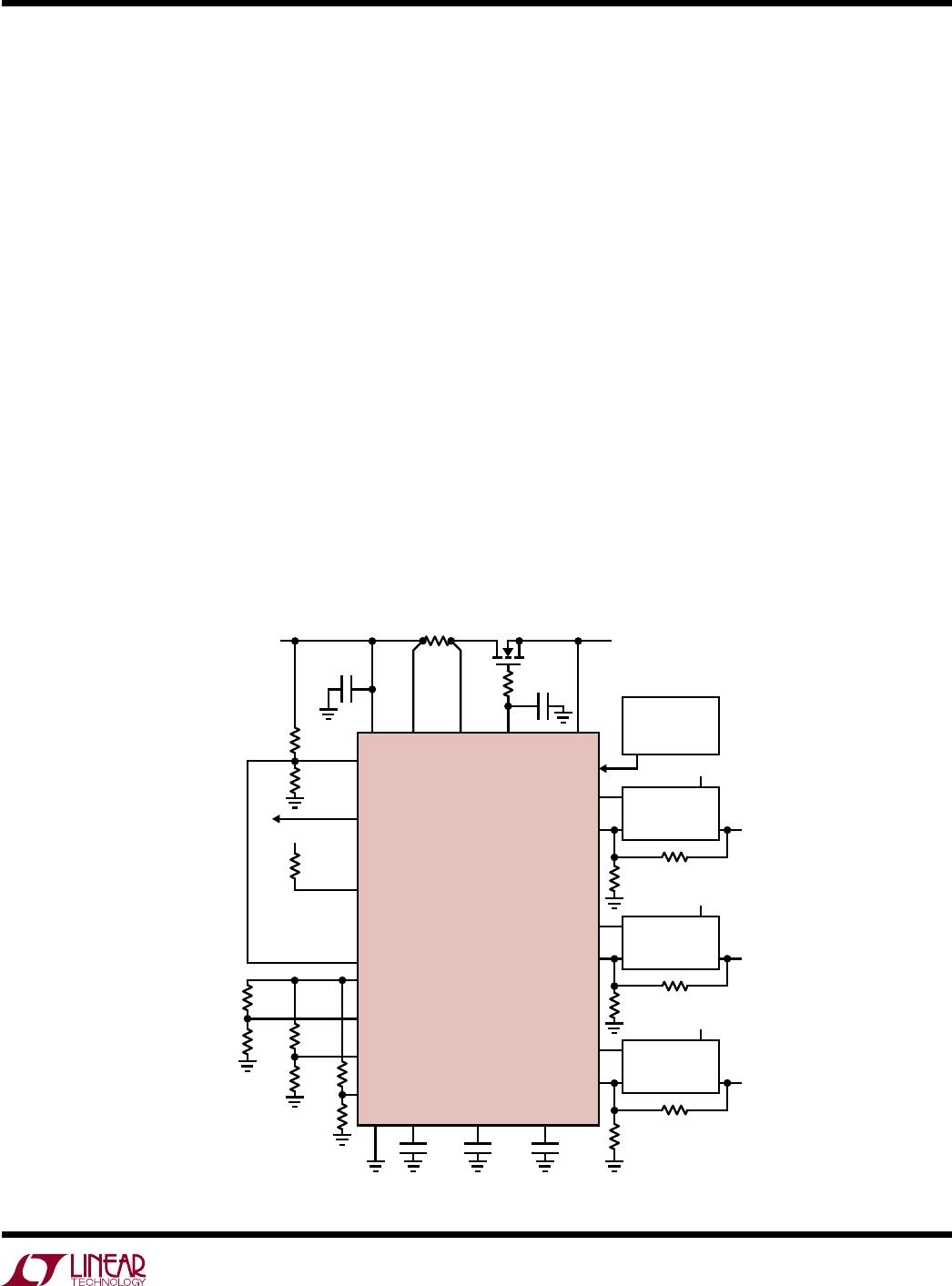
application circuit is shown in Figure 10.
1.
Set the ramp rate of the master signal.
Solve for the value of C
GATE
, the capacitor on the GATE
pin, based on the desired ramp rate (V/s) of the master
supply, S
M
:
C
S
whereIA
GATE
GATE
GATE
=≈μ10 1
If the external FET has a gate capacitance comparable
to C
GATE
, then the external capacitor’s value should be
reduced to compensate for the FET’s gate capacitance.
If no external FET is used, tie the GATE and RAMP pins
together, connect SENSEN and SENSEP to V
CC
, and con-
nect SCTMR to GND.
2. So
lve for the pair of resistors that provide the desired
ramp rate of the slave supply, assuming no delay.
Choose a ramp rate for the slave supply, S
S
. If the slave
supply ramps up coincident with the master supply or
with a fixed voltage offset, then the ramp rate equals the
master supply’s ramp rate. Be sure to use a fast enough
ramp rate for the slave supply so that it will finish ramping
before the master supply has reached its final supply value.
If not, the slave supply will be held below the intended
regulation value by the master supply. Use the following
formulas to determine the resistor values for the desired
ramp rate, where R
FB
and R
FA
are the feedback resistors in
the slave supply and V
FB
is the feedback reference voltage
of the slave supply:
RR
S
TB FB
M
=
)2
R
V
R
V
R
V
R
TA
TRACK
FB
FB
TRACK
ʹ=
+ –
3
where V
TRACK
≈ 0.8V.
Note that large ratios of slave ramp rate to master ramp
rate, S
S
/S
M
, may result in negative values for R
TA
´. If a
sufficiently large delay is used in step 3, R
TA
will be posi-
tive, otherwise S
S
/S
M
must be reduced.
3. Choose R
TA
to obtain the desired delay.
If no delay is required, such as in coincident and ratiometric
tracking, then simply set R
TA
= R
TA
´. If a delay is desired,
as in offset tracking and supply sequencing, calculate R
TA
´´
to determine the value of R
TA
where t
D
is the desired delay.
R
tS
TA
TRACK TB
ʹʹ =
•
4
=ʹ ʹʹ
the parallel combination of R
TA
´ and R
TA
´´.
As noted in step 2, small delays and large ratios of slave
ramp rate to master ramp rate (usually only seen in se
-
quencing) may result in solutions with negative values for
R
TA
. In such cases, either the delay must be increased or
the ratio of slave ramp rate to master ramp rate must be
reduced.
applicaTions inForMaTion
R
SENSE
Q1
0.1µF
10k
V
CC
SENSEP SENSEN
V
IN
V
IN
V
IN
R
ONB
138k
V
IN
R
TB1
R
TB2
R
FA2
SLAVE2
MASTER
R
FB2
R
TA2
R
TB3
R
TA3
R
TA1
R
ONA
100k
RAMPBUF
TRACK1
TRACK2
TRACK3
FB2
GATE
LTC2925
PGTMR
SDTMRSCTMRGND
2925 F10
RAMP
R
FA3
SLAVE3
R
FB3
DC/DC
IN
FB OUT
DC/DC
IN
FB
RUN/SS
RUN/SS
OUT
FB3
V
IN
PGI
R
FA1
SLAVE1
R
FB1
SUPPLY
MONITOR
DC/DC
IN
FB
RUN/SS
OUT
FB1
FAULT
ON
10k
V
IN
STATUS
REMOTE
RST
SD3
SD2
SD1
C
GATE
10Ω
Figure 10. Four Supply Application