MAX3541
Application Information
RF Inputs
The MAX3541 features separate UHF and VHF inputs
that are matched to 75Ω. Both inputs require a DC-
blocking capacitor. The active inputs are selected by
the input registers. In addition, the input registers
enable or disable the lowpass filter, which can be used
when the VHF input is selected. For the 47MHz to
68MHz, select the VHF_IN with the LPF filter enabled
(INPT = 00). For 174MHz to 230MHz, select VHF_IN
with LPF disabled (INPT = 01). For 470MHz to 862MHz,
select UHF_IN (INPT = 10).
RF Gain Control
The gain of the RF low-noise amplifier can be adjusted
over a typical range of 45dB with the RFAGC pin. The
RFAGC input accepts a DC voltage from 0.5V to 3V,
with 3V providing maximum gain. This pin can be con-
trolled with the IF power-detector output to form a
closed RF gain-control loop. See the
Closed-Loop RF
Gain Control
section for more information.
RF Tracking Filter
The MAX3541 includes a programmable tracking filter
for each band of operation to optimize rejection of
out-of-band interference while minimizing insertion
loss for the desired received signal. The center fre-
quency of each tracking filter is selected by a
switched-capacitor array that is programmed by the
TFS[7:0] bits in the Tracking Filter Series Capacitor
register and the TFP[5:0] bits in the Tracking Filter
Parallel Cap register.
Optimal tracking filter settings for each channel varies
from part to part due to process variations. To accom-
modate part-to-part variations, each part is factory cal-
ibrated by Maxim. During calibration, the y-intercept
and slope for the series and parallel tracking capacitor
arrays is calculated and written into an internal ROM
table. The user must read the ROM table upon power-
up and store the data in local memory (8 bytes total) to
calculate the optimal TFS[7:0] and TFP[5:0] settings
for each channel. Table 16 shows the address and
bits for each ROM table entry. See the
Interpolating
Tracking Filter Coefficients
section for more informa-
tion on how to calculate the required values.
Reading the ROM Table
Each ROM table entry must be read using a two-step
process. First, the address of the ROM bits to be read
must be programmed into the TFA[3:0] bits in the
Tracking Filter ROM Address register (Table 11).
Complete Single-Conversion
Television Tuner
16 ______________________________________________________________________________________
MSB LSB
DATA BYTE
DESCRIPTION ADDRESS
D7 D6 D5 D4 D3 D2 D1 D0
Reserved 0x0 OD2 OD1 OD0 X X X X X
VHF Series
Y-Intercept
0x1 VS0[7] VS0[6] VS0[5] VS0[4] VS0[3] VS0[2] VS0[1] VS0[0]
VHF Series
Slope
0x2 VS1[7] VS1[6] VS1[5] VS1[4] VS1[3] VS1[2] VS1[1] VS1[0]
VHF Parallel
Y-Intercept
0x3 VP0[7] VP0[6] VP0[5] VP0[4] VP0[3] VP0[2] VP0[1] VP0[0]
VHF Parallel
Slope
0x4 VP1[7] VP1[6] VP1[5] VP1[4] VP1[3] VP1[2] VP1[1] VP1[0]
UHF Series
Y-Intercept
0x5 US0[7] US0[6] US0[5] US0[4] US0[3] US0[2] US0[1] US0[0]
UHF Series
Slope
0x6 US1[7] US1[6] US1[5] US1[4] US1[3] US1[2] US1[1] US1[0]
UHF Parallel
Y-Intercept
0x7 UP0[7] UP0[6] UP0[5] UP0[4] UP0[3] UP0[2] UP0[1] UP0[0]
UHF Parallel
Slope
0x8 UP1[7] UP1[6] UP1[5] UP1[4] UP1[3] UP1[2] UP1[1] UP1[0]
Table 16. ROM Table
Once the address has been programmed, the data
stored in that address is transferred to the TFR[7:0] bits
in the ROM Table Data Readback register (Table 13).
The ROM data at the specified address can then be
read from the TFR[7:0] bits and stored in the micro-
processor’s local memory.
Interpolating Tracking Filter Coefficients
The TFS[7:0] and TFP[5:0] bits must be reprogrammed
for each channel frequency to optimize performance.
The optimal settings for each channel can be calculat-
ed from the ROM table data using the equations below:
VHF filter:
UHF filter:
:
where:
f
RF
= operating frequency in megahertz.
TFS = decimal value of the optimal TFS[7:0] setting
(Table 9) for the given operating frequency.
TFP = decimal value of the optimal TFP[5:0] setting
(Table 10) for the given operating frequency.
VS0, VS1, VP0, VP1, US0, US1, UP0, and UP1 = the
decimal values of the ROM table coefficients (Table
16).
IF Overload Detector
The MAX3541 includes a broadband IF overload detec-
tor, which provides an indication of the total power pre-
sent at the RF input. The overload-detector output voltage
is compared to a reference voltage, and the difference is
amplified. This error signal drives an open-collector tran-
sistor whose collector is connected to the IFOVLD pin,
causing the IFOVLD pin to sink current. The nominal full-
scale current sunk by the IFOVLD pin is 300μA. The
IFOVLD pin requires a 10kΩ pullup resistor to V
CC
.
The IF overload detector is calibrated at the factory to
attack at 0.7V
P-P
at the IFOUT1. Upon power-up, the
baseband processor must read OD[2:0] from the ROM
table and store it in the IFVOLD register.
Closed-Loop RF Gain Control
Closed-loop RF gain control can be implemented by
connecting the IFOVLD output to the RFAGC input.
Using a 10kΩ pullup resistor on the IFOVLD pin as
shown in the
Typical Application Circuit
results in a
nominal control voltage range of 0.5V to 3V.
VCO and VCO Divider Selection
The MAX3541 frequency synthesizer includes three
VCOs and eight VCO sub-bands to guarantee a
2200MHz to 4400MHz VCO frequency range. The fre-
quency synthesizer also features an additional VCO fre-
quency divider that must be programmed to either 4, 8,
16, or 32 by the VDIV[1:0] bits in the VCO register based
on the channel being received.
To ensure PLL lock, the proper VCO and VCO sub-band
for the channel being received must be chosen by itera-
tively selecting a VCO and VCO sub-band, then reading
the LD[2:0] bits to determine if the PLL is locked. Any
reading from 001 to 110 indicates the PLL is locked. If
LD[2:0] reads 000, the PLL is unlocked and the selected
VCO is at the bottom of its tuning range; a lower VCO
sub-band must be selected. If LD[2:0] reads 111, the PLL
is unlocked and the selected VCO is at the top of its tun-
ing range; a higher VCO sub-band must be selected. The
VCO and VCO sub-band settings should be progressive-
ly increased or decreased until the LD[2:0] reading falls in
the 001 to 110 range.
Due to overlap between VCO sub-band frequencies, it is
possible that multiple VCO settings can be used to tune
to the same channel frequency. System performance at
a given channel should be similar between the various
possible VCO settings, so it is sufficient to select the first
VCO and VCO sub-band that provides lock.
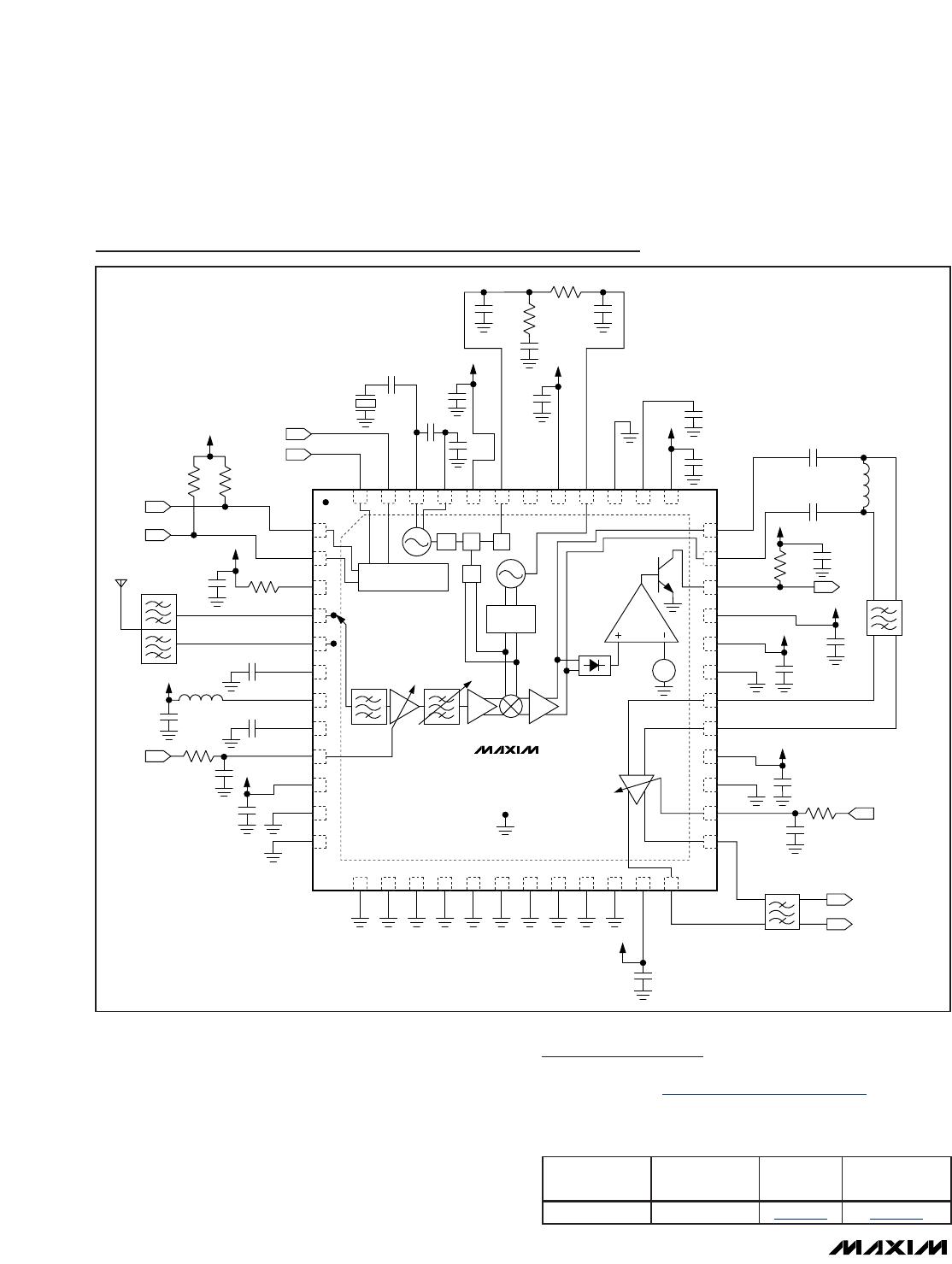
Layout Considerations
The MAX3541 EV kit can serve as a guide for PCB lay-
out. Keep RF signal lines as short as possible to mini-
mize losses and radiation. Use controlled impedance on
all high-frequency traces. The exposed paddle must be
soldered evenly to the board’s ground plane for proper
operation. Use abundant vias beneath the exposed pad-
dle for maximum heat dissipation. Use abundant ground
vias between RF traces to minimize undesired coupling.
To minimize coupling between different sections of the
IC, the ideal power-supply layout is a star configuration,
which has a large decoupling capacitor at the central
V
CC
node. The V
CC
traces branch out from this node,
with each trace going to separate V
CC
pins of the
MAX3541. Each V
CC
pin must have a bypass capacitor
with a low impedance to ground at the frequency of
interest. Do not share ground vias among multiple con-
nections to the PCB ground plane.
TFS INT[10
[
US0
256
5
US1
256
-1) 5
=
×+ ××( 110 f ]
[
UP0
256
5
UP
-3
RF
]10
TFP INT[10
×
×+
=
(
11
256
-1) 5 10 f ]
-3
RF
]
×× ×
TFS 10
[
VS0
256
5
VS1
256
-1) 1.5
=
×+ ×
INT[
( ×××
×+
=
10 f ]
[
VP0
256
5
VP1
2
-2
RF
TFP INT[10
]
(
556
-1) 10 f ]
-2
RF
]
××
MAX3541
Complete Single-Conversion
Television Tuner
______________________________________________________________________________________ 17
MAX3541
Complete Single-Conversion
Television Tuner
18 ______________________________________________________________________________________
MAX3541
36
IFOUT1-
1
13
48
14
47
15
46
16
45
17
44
18
43
19
42
20
41
21
40
22
39
23
38
24
37
SCL
35
IFOUT1+
2
SDA
34
IFOVLD
3
V
CC
33
V
CC
4
UHF_IN
32
V
CC
V
REF
5
VHF_IN
31
GND
6
RFGND2
30
IFIN+
7
LEXT
29
IFIN-
8
RFGND3
28
V
CC
9
RFAGC
27
GND
10
V
CC
26
IFAGC
11
GND
25
IFOUT2+
12
GND
1000pF
ADDR2GND
ADDR1GND
XTALPGND
XTALNGND
V
CC
GND
CPGND
MUXGND
V
CC
GND
VTUNEGND
GND_TUNEGND
LDOV
CC
V
CC
IFOUT2-
SERIAL
INTERFACE
÷ R PD CP
÷ N
VCO
DIVIDER
ANTI-ALIASING
FILTER
2.7kΩ
1000pF
1000pF
EP
+
-
IFOUT+
V
IFAGC
IFOUT-
IFOVLD
V
CC
0.1μF
1000pF
0.1μF
V
CC
1000pF
10kΩ
V
CC
1000pF
V
CC
1000pF
V
CC
1000pF
1000pF
2.7kΩ
2.7kΩ2.7kΩ
IFOVLD
0.1μF
1000pF
47μF
100Ω
820pF 560pF
0.033μF
2.2kΩ
V
CC
IF-SAW
FILTER
680nH
1000pF
1000pF
22pF
8MHz
4.3kΩ
220pF
220pF
270nH
1000pF
V
CC
V
CC
SDATA
SCLK
ADDRESS 2
ADDRESS 1
V
CC
V
CC
V
CC
**
**
**
**
1000pF
V
CC
** CONNECT TO COMMON GROUND POINT AT PIN 39
Typical Application Circuit
Package Information
For the latest package outline information and land patterns
(footprints), go to www.maxim-ic.com/packages. Note that a
“+”, “#”, or “-” in the package code indicates RoHS status only.
Package drawings may show a different suffix character, but
the drawing pertains to the package regardless of RoHS status.
PACKAGE
TYPE
PACKAGE
CODE
OUTLINE
NO.
LAND
PATTERN NO.
48 LGA-EP L4877F+15
21-0152 90-0303

MAX3541ELM+

Mfr. #:
Manufacturer:
Maxim Integrated
Description:
Tuners Single-Conversion Television Tuner
Lifecycle:
New from this manufacturer.
Delivery:
DHL FedEx Ups TNT EMS
Payment:
T/T Paypal Visa MoneyGram Western Union

Products related to this Datasheet