Features
n Superior circuit protection
n Overcurrent and overvoltage protection
n Blocks surges up to rated limits
n High-speed performance
n Small SMT package
n RoHS compliant*
n Agency listing:
Applications
n Ethernet ports
n Protection modules and dongles
n Process control equipment
n Test and measurement equipment
n General electronics
TBU-DT Series - TBU
®
High-Speed Protectors
General Information
The TBU-DT Series of Bourns
®
TBU
®
(Transient Blocking Unit) products are very low
capacitance dual unidirectional high-speed surge protection components designed to
protect against faults caused by short circuits, AC power cross, induction and lightning
surges.
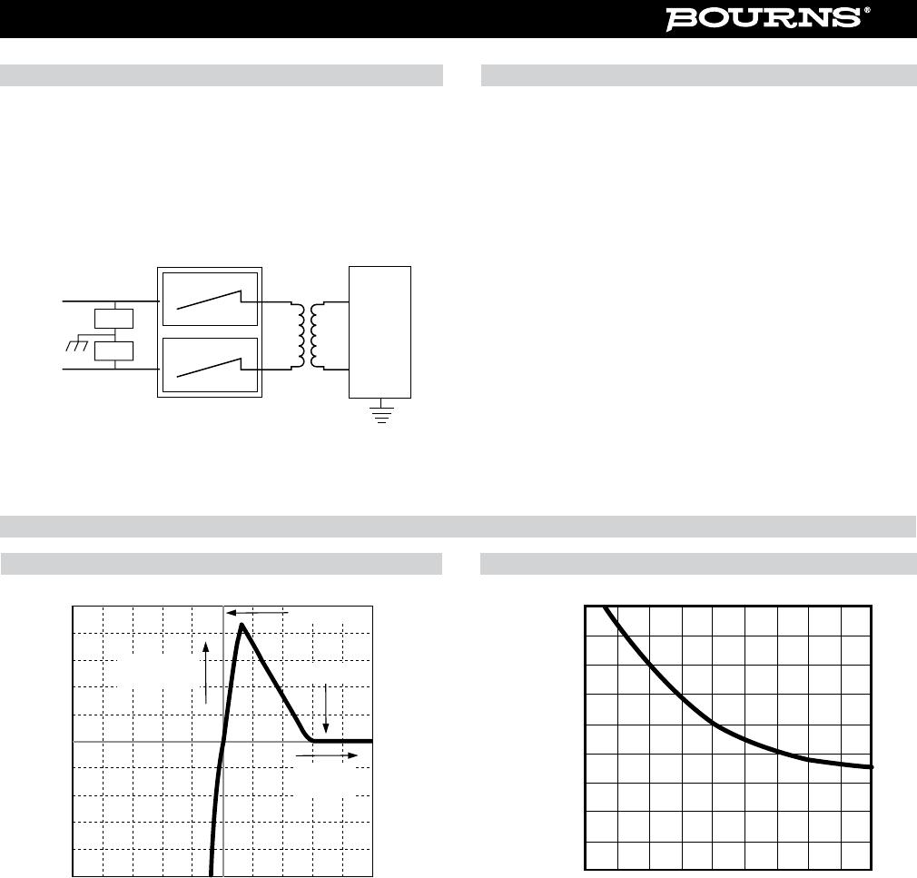
The TBU-DT series is a unidirectional TBU
®
device; the TBU
®
protector will trip in less
than 1 ms when the current reaches the maximum value in one direction only, that is when
Pin 1 is positive in voltage with respect to Pin 2, and Pin 4 is positive with respect to Pin 3.
No current limiting exists in the opposite polarity, and the TBU
®
device appears as resis-
tive in nature. The reverse current should not exceed the maximum trigger current level of
the TBU
®
device. An external diode may be used to prevent reverse current in DC biased
applications.
The TBU
®
protector blocks surges and provides an effective barrier behind which sensitive
electronics will not be exposed to large voltages or currents during surge events. After the
surge, the TBU
®
device resets when the voltage across the TBU
®
device falls to the V
reset
level. The TBU
®
device will automatically reset on lines which have no DC bias or have
DC bias below Vreset (such as unpowered signal lines).
The TBU
®
device is provided in a surface mount DFN package and meets industry
standard requirements such as RoHS and Pb Free solder reow proles.
Agency Listing
Description
UL File Number: E315805
Absolute Maximum Ratings (@ T
A
= 25 °C Unless Otherwise Noted)
Symbol Parameter Part Number Value Unit
V
imp
Peak impulse voltage withstand with duration less than 10 ms
TBU-DT065-xxx-WH
TBU-DT085-xxx-WH
650
850
V
V
rms
Continuous A.C. RMS voltage
TBU-DT065-xxx-WH
TBU-DT085-xxx-WH
300
425
V
T
op
Operating temperature range -40 to +125 °C
T
stg
Storage temperature range -65 to +150 °C
Electrical Characteristics (@ T
A
= 25 °C Unless Otherwise Noted)
Symbol Parameter Part Number Min. Typ. Max. Unit
I
trigger
Current required for the device to go from operating state to
protected state
TBU-DTxxx-100-WH
TBU-DTxxx-200-WH
TBU-DTxxx-300-WH
TBU-DTxxx-500-WH
100
200
300
500
150
300
450
750
200
400
600
1000
mA
R
device
Series resistance of
the TBU
®
device
V
imp
= 650 V I
trigger
(min.) = 100 mA
V
imp
= 650 V I
trigger
(min.) = 200 mA
V
imp
= 650 V I
trigger
(min.) = 300 mA
V
imp
= 650 V I
trigger
(min.) = 500 mA
V
imp
= 850 V I
trigger
(min.) = 100 mA
V
imp
= 850 V I
trigger
(min.) = 200 mA
V
imp
= 850 V I
trigger
(min.) = 300 mA
V
imp
= 850 V I
trigger
(min.) = 500 mA
TBU-DT065-100-WH
TBU-DT065-200-WH
TBU-DT065-300-WH
TBU-DT065-500-WH
TBU-DT085-100-WH
TBU-DT085-200-WH
TBU-DT085-300-WH
TBU-DT085-500-WH
8.5
5.6
4.6
4.0
10.3
7.4
6.5
5.8
10.0
6.6
5.6
4.8
12.1
8.7
7.7
6.9
Ω
R
match
Package resistance matching of the TBU
®
device #1 - TBU
®
device #2 -0.5 +0.5
Ω
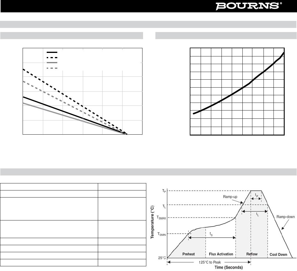
t
block
Time for the device to go from normal operating state to protected state 1 µs
I
Q
Current through the triggered TBU
®
device
with 50 Vdc circuit voltage 0.25 0.50 1.00 mA
V
reset
Voltage below which the triggered TBU
®
device will transition to normal operating state 10 14 18 V
R
th(j-l)
Junction to package pads - FR4 using recommended pad layout 116 °C/W
R
th(j-l)
Junction to package pads - FR4 using heat sink on board (6 cm
2
) 96 °C/W
TBU
®
Device
Line Side
12
Load Side
Line Side
43
Load Side
*RoHS COMPLIANT
LEAD FREE
*RoHS COMPLIANT
VERSIONS
AVAILABLE
LEAD FREE
VERSIONS ARE
RoHS COMPLIANT*
*RoHS Directive 2002/95/EC Jan. 27, 2003 including annex and RoHS Recast 2011/65/EU June 8, 2011.
Specifications are subject to change without notice.
The device characteristics and parameters in this data sheet can and do vary in different applications and actual device performance may vary over time.
Users should verify actual device performance in their specific applications.